
Reverse Engineering the Nvidia SXM2 Socket
Note: all the files are hosted in a Github repo
For another project, it was necessary for me to acquire the pinout for Nvidia’s SXM2 socket. This is a high-bandwidth mezzanine connector used in Nvidia datacenter GPUs. The SXM2 “standard” is quite old at the time of this writing (mid-2025), but details of this connector, including a pinout or even mechanical drawings, are still locked under NDAs at Nvidia’s behest.
Therefore, to get the details on this pinout, I had to do it the old-fashioned way. I had to reverse engineer it.
The basis of this reverse engineering came from a PCIe SXM2 carrier board that can be found on the Chinese parts of the internet. My carrier board is effectively identical to this carrier board purchased by l4rz. It contains everything needed: an SXM2 footprint with a single Amphenol Meg-Array connector, and power is delivered by two 2x3 PCIe power headers. There’s some circuitry on the back for a fan PWM controller, but not much else. The NVLink connector – the second Meg-Array connector – is not populated, because this card is only meant for a single SXM2 module.
Because of the simplicity of this circuit, it really is mostly only a matter of testing the continuity of all the pins with a multimeter. Mostly.
The Pinout
__Again, all of the files needed to build your own SXM2 to PCIe adapter are in a Github repo.__
This is, to the best of my ability, the pinout for an SXM2 module:
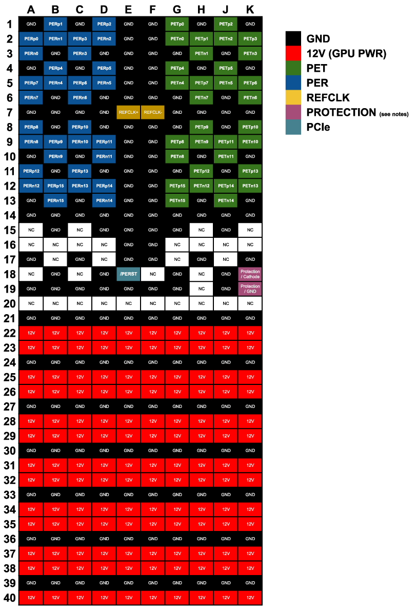
Also in table format:
📑 Full SXM2 pin map (40 × 10) – click to view
| Row | A | B | C | D | E | F | G | H | J | K |
|---|---|---|---|---|---|---|---|---|---|---|
| 1 | GND | PERp1 | GND | PERp2 | GND | GND | PETp0 | GND | PETp2 | GND |
| 2 | PERp0 | PERn1 | PERp3 | PERn2 | GND | GND | PETn0 | PETp1 | PETn2 | PETp3 |
| 3 | PERn0 | GND | PERn3 | GND | GND | GND | GND | PETn1 | GND | PETn3 |
| 4 | GND | PERp4 | GND | PERp5 | GND | GND | PETp4 | GND | PETp5 | GND |
| 5 | PERp7 | PERn4 | PERp6 | PERn5 | GND | GND | PETn4 | PETp7 | PETn5 | PETp6 |
| 6 | PERn7 | GND | PERn6 | GND | GND | GND | GND | PETn7 | GND | PETn6 |
| 7 | GND | GND | GND | GND | REFCLK+ | REFCLK- | GND | GND | GND | GND |
| 8 | PERp8 | GND | PERp10 | GND | GND | GND | GND | PETp9 | GND | PETp10 |
| 9 | PERn8 | PERp9 | PERn10 | PERp11 | GND | GND | PETp8 | PETn9 | PETp11 | PETn10 |
| 10 | GND | PERn9 | GND | PERn11 | GND | GND | PETn8 | GND | PETn11 | GND |
| 11 | PERp12 | GND | PERp13 | GND | GND | GND | GND | PETp12 | GND | PETp13 |
| 12 | PERn12 | PERp15 | PERn13 | PERp14 | GND | GND | PETp15 | PETn12 | PETp14 | PETn13 |
| 13 | GND | PERn15 | GND | PERn14 | GND | GND | PETn15 | GND | PETn14 | GND |
| 14 | GND | GND | GND | GND | GND | GND | GND | GND | GND | GND |
| 15 | NC | GND | NC | GND | GND | GND | GND | NC | GND | NC |
| 16 | NC | NC | NC | NC | GND | GND | NC | NC | NC | NC |
| 17 | GND | NC | GND | NC | GND | GND | NC | GND | NC | GND |
| 18 | NC | GND | NC | GND | /PERST | NC | GND | NC | GND | Prot/Cathode |
| 19 | GND | GND | GND | GND | GND | GND | GND | NC | GND | Prot/GND |
| 20 | NC | NC | NC | NC | NC | NC | NC | NC | NC | NC |
| 21 | GND | GND | GND | GND | GND | GND | GND | GND | GND | GND |
| 22 | 12V | 12V | 12V | 12V | 12V | 12V | 12V | 12V | 12V | 12V |
| 23 | 12V | 12V | 12V | 12V | 12V | 12V | 12V | 12V | 12V | 12V |
| 24 | GND | GND | GND | GND | GND | GND | GND | GND | GND | GND |
| 25 | 12V | 12V | 12V | 12V | 12V | 12V | 12V | 12V | 12V | 12V |
| 26 | 12V | 12V | 12V | 12V | 12V | 12V | 12V | 12V | 12V | 12V |
| 27 | GND | GND | GND | GND | GND | GND | GND | GND | GND | GND |
| 28 | 12V | 12V | 12V | 12V | 12V | 12V | 12V | 12V | 12V | 12V |
| 29 | 12V | 12V | 12V | 12V | 12V | 12V | 12V | 12V | 12V | 12V |
| 30 | GND | GND | GND | GND | GND | GND | GND | GND | GND | GND |
| 31 | 12V | 12V | 12V | 12V | 12V | 12V | 12V | 12V | 12V | 12V |
| 32 | 12V | 12V | 12V | 12V | 12V | 12V | 12V | 12V | 12V | 12V |
| 33 | GND | GND | GND | GND | GND | GND | GND | GND | GND | GND |
| 34 | 12V | 12V | 12V | 12V | 12V | 12V | 12V | 12V | 12V | 12V |
| 35 | 12V | 12V | 12V | 12V | 12V | 12V | 12V | 12V | 12V | 12V |
| 36 | GND | GND | GND | GND | GND | GND | GND | GND | GND | GND |
| 37 | 12V | 12V | 12V | 12V | 12V | 12V | 12V | 12V | 12V | 12V |
| 38 | 12V | 12V | 12V | 12V | 12V | 12V | 12V | 12V | 12V | 12V |
| 39 | GND | GND | GND | GND | GND | GND | GND | GND | GND | GND |
| 40 | 12V | 12V | 12V | 12V | 12V | 12V | 12V | 12V | 12V | 12V |
The Temperature Sensor That Wasn’t
Apart from the fan controller circuitry on the back of the card, there is one other small piece of active electronics on this card: a mysterious SOT-23-3 component positioned right behind the PCIe Meg-Array connector.
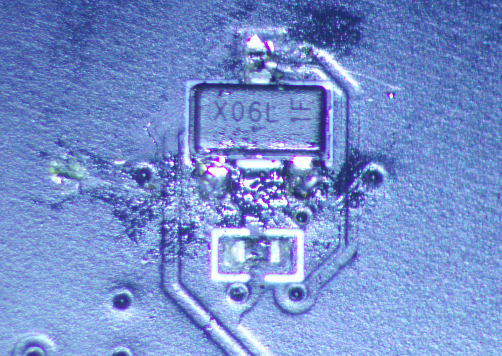
At first glance, the circuit topology was deceiving. An SOT-23-3 package with a 10k pull-up resistor to 3.3V, connected to undocumented SXM2 pins K18 and K19? My initial assumption was a temperature sensor - perhaps an analog output thermistor or similar monitoring device. The pinout seemed to match: power, ground, and output.
The component bears the marking “X06L” with “1F” rotated 90 degrees - a code that doesn’t appear in any of the standard SMD marking databases, including smdmarkingcodes.com or LCSC’s extensive catalog. Without documentation, I had to resort to reverse engineering.
Initial testing: it’s not a temperature sensor
My first round of testing quickly disproved the temperature sensor theory. With the component powered in-circuit, I subjected it to temperature extremes - ice cubes and hot air at 100°C - with no change in output voltage. What I did discover was far more interesting: the output voltage tracked the input voltage with a consistent ~0.4V drop:
- 2.5V In -> 2.13V Out
- 3.3V In -> 2.93V Out
- 3.9V In -> 3.5V Out
This behavior immediately suggested a diode, not an active component.
Detailed Characterization
After desoldering the component for thorough testing, I confirmed my suspicions. Diode mode measurements revealed:
- Pin 2 to Pin 3: 0.54V forward drop
- All other pin combinations: Open circuit
- Pin 1: Completely unconnected internally
This is the unmistakable signature of a single diode in an SOT-23-3 package, where pin 1 serves only as a mechanical support. To identify the specific type, I performed a forward voltage vs. current characterization:
| Resistor Value | Measured VF | Calculated Current | Notes |
|---|---|---|---|
| 33kΩ | 0.482V | 0.085mA | Very low current |
| 3.3kΩ | 0.521V | 0.842mA | Close to 1mA |
| 680Ω | 0.549V | 4.049mA | ~4mA |
| 330Ω | 0.563V | 8.294mA | ~8mA |
| 150Ω | 0.576V | 18.16mA | ~18mA |
The key observations is a very low forward voltage, highly suggesting a BAT54 series Schottky diode.
These measurements perfectly match the characteristics of a low VF Schottky diode, most likely a BAT54 or equivalent. The “X06L” marking is almost certainly a house code from a Chinese manufacturer for this common jellybean part.
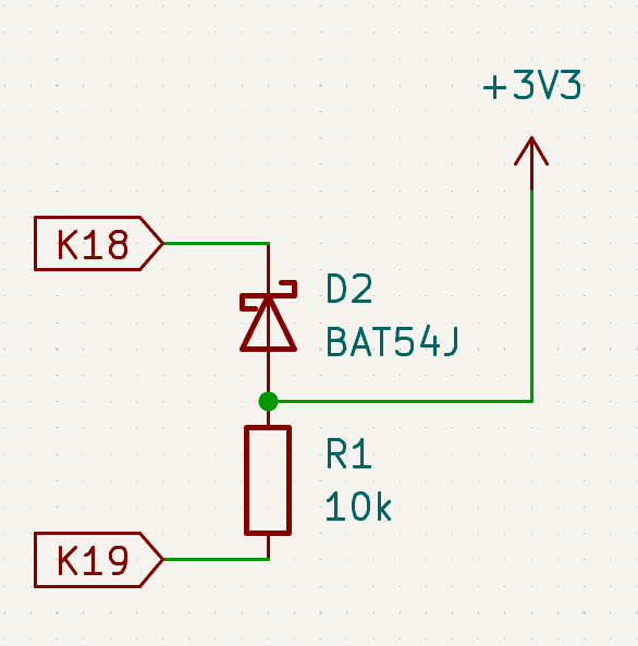
Circuit Function
The actual circuit is elegantly simple: a Schottky diode drops the 3.3V auxiliary power from the PCIe slot by ~0.4V before feeding it to the SXM2 module’s K18 pin. The 10k resistor provides a pull-up to ensure a defined state when unpowered. Without NVIDIA’s proprietary SXM2 documentation, the exact purpose remains speculative, but likely candidates include protection, preventing reverse current flow from the GPU module, or signal conditioning, creating a logic level offset for internal monitoring.
For anyone repairing these adapters, a BAT54 Schottky diode in SOT-23-3 package is a perfect replacement. Connect it with the anode to the 10k resistor node and cathode to K18, leaving pin 1 unconnected. The specific variant (BAT54S, BAT54A, etc.) doesn’t matter as long as it has similar forward voltage characteristics.
Finding the correct part
Even though I can characterize this part and infer its function – as well as make a reasonable copy of it for my own board – I still can not find a drop-in compatible replacement. The standard BAT54 from Vishay, in SOT-23-3 packaging, has Pin 2 as NC, Pin 1 as the Anode, and Pin 3 as the Cathode. My part has Pin 1 as NC, Pin 2 as the Anode, and Pin 3 as the Cathode. A complete search of Schottkys on LCSC returned no parts that match this configuration. As such, I opted to replace the mystery SOT-23 package with a two-pin SOD-123 package (LCSC Part C549277). The schematic I’m using is below:
If you know this isn’t correct or have a better idea, PRs are welcome on this project’s Github.
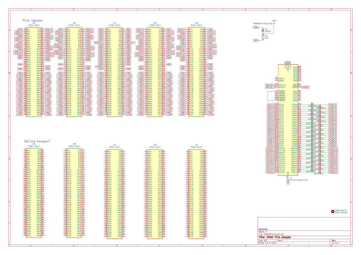
The Actual Schematic
After mapping GND, 12V, the PCIe lanes, and the mysterious circuit, there were 32 unconnected pins in the Meg-Array connector, in rows 15 through 20, with the entirety of row 20 being disconnected. This required much more thorough investigations and continuity tracing. The PERST# signal was found on E18, but no JTAG or other connections were found.
Interesting things of note: The SMBUS/I2C signals on the PCIe connector are unconnected, as are the JTAG signals. I don’t know what to tell you about this, except I know this card works, therefore my reverse engineering attempt should. There is no 3.3V rail from the PCIe card going to the SXM2 socket. Again, your guess is as good as mine. That leaves 31 individual pins in the SXM connector unmapped, or probably unconnected. I do not know where these pins lead, although they probably connect to the other Meg-Array for the NVLink signals.
Other than the connections from the SXM module to the PCIe card edge, there is another, single connection in between PCIe card pins: The PRSNT1# must connect to the farthest PRSNT2# pin. Since this is an x16 card, this means pin A1 is connected to pin B81.
The following is the complete schematic, with files also available on my Github:
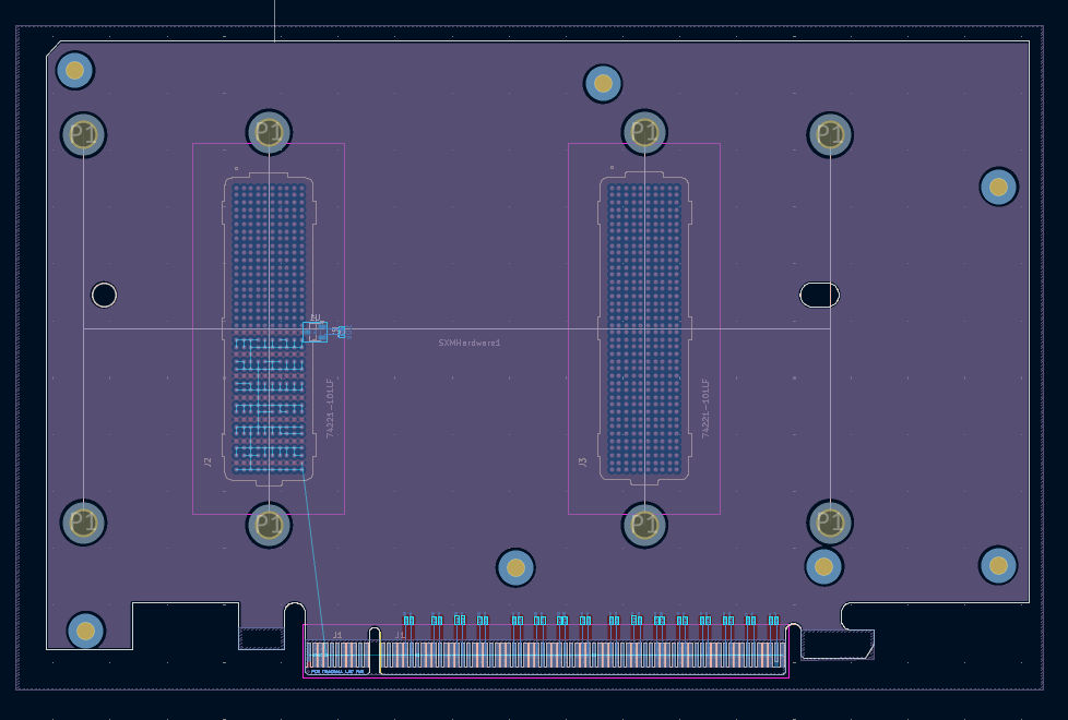
The Mechanical Footprint
Finally, the mechanical part of the build. The actual footprint.
The footprint itself is just two Meg-Array connectors, but one is left unpopulated. Easy enough. The hard part is the mechanical portion. The SXM2 module is fastened to the board with eight individual M3 screws. These are M3 SMD standoffs, soldered to the opposite side of the board. Other than that, it’s a standard PCIe x16 card.
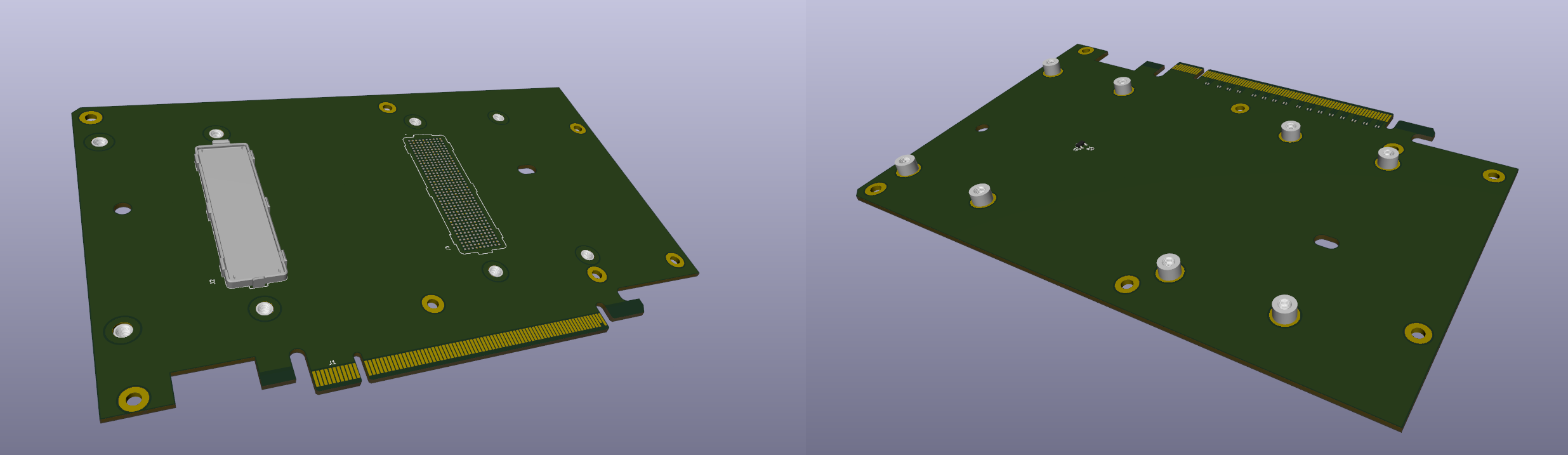
Because I don’t have a coordinate measuring machineor optical comparator in my pocket, I used a pair of digital calipers to measure the footprint of all the features of the board. By carefully referencing all of the measurements from the SMD M3 standoffs (and between the standoffs themselves), I eventually got the correct footprint. This, surprisingly, worked. All of the features of my SXM2 socket mate with the SXM2 module. You can do a lot with a pair of digital calipers.
Routing
All work for this project is available on my Github.
License
Text © 2025 Brian Benchoff, released under CC-BY-SA-4.0.
Hardware design files: WTFPL 3.0, MODIFIED FOR NERDS (see LICENSE in the repo).