

OrthoRoute — GPU-Accelerated Autorouting for KiCad
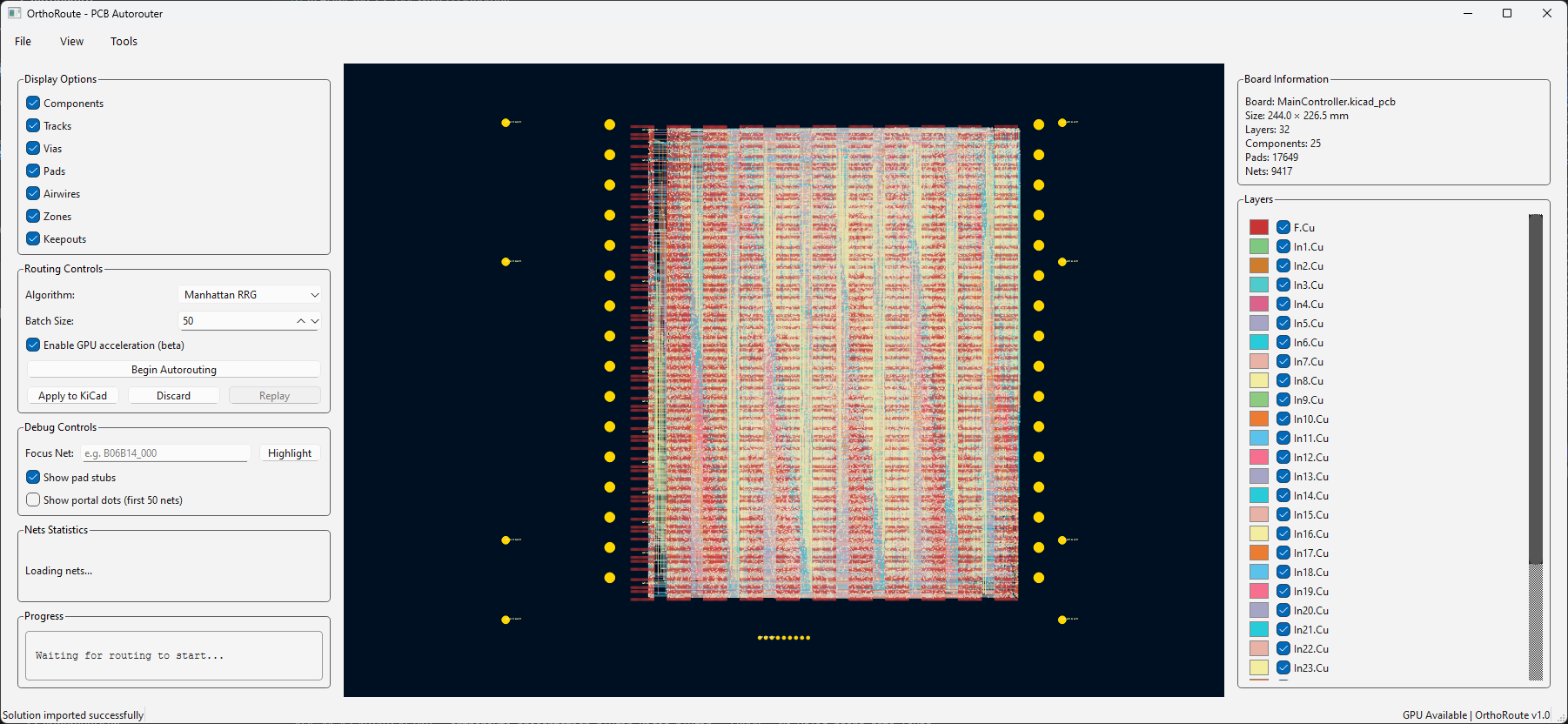
OrthoRoute is a GPU-accelerated PCB autorouter that uses a Manhattan lattice and the PathFinder algorithm to route high-density boards. Built as a KiCad plugin using the IPC API, it handles complex designs with thousands of nets that make traditional push-and-shove routers give up.
Never trust the autorouter, but at least this one is fast.
This document is a complement to the README in the Github repository. The README provides information about performance, capabilities, and tests. This document reflects more on the why and how OrthoRoute was developed.
Why I Built This
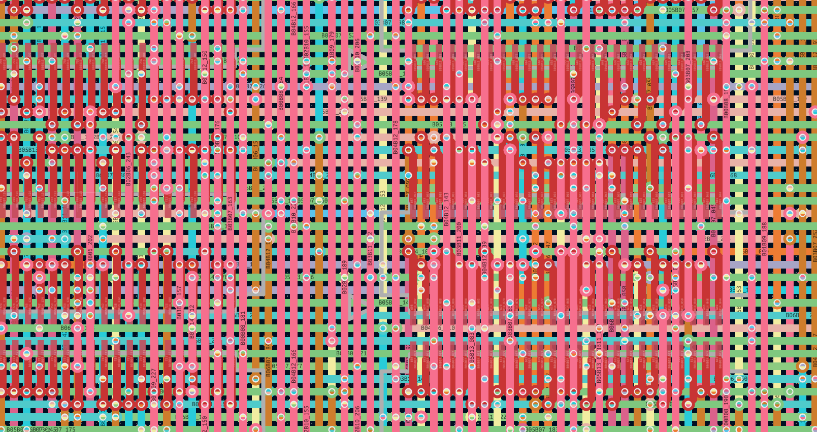
This is a project born out of necessity. Another thing I was working on needed an enormous backplane. A PCB with sixteen connectors, with 1,100 pins on each connector. That’s 17,600 individual pads, and 8,192 airwires that need to be routed. Here, just take a look:
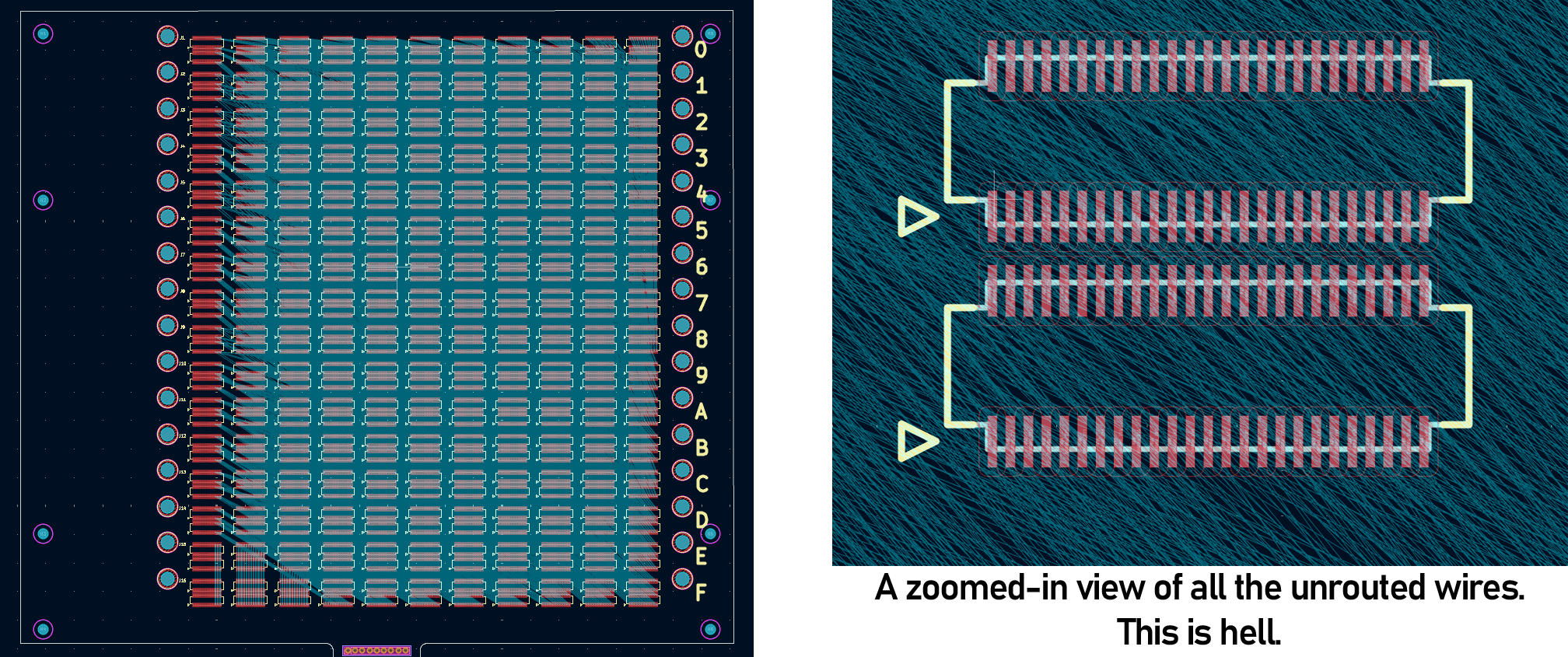
Look at that shit. Hand routing this would take months. For a laugh, I tried FreeRouting, the KiCad autorouter plugin, and it routed 4% of the traces in seven hours. If that trend held, which it wouldn’t, that would be a month of autorouting. And it probably wouldn’t work in the end. I had a few options, all of which would take far too long
- I could route the board by hand. This would be painful and take months, but I would get a good-looking board at the end.
- I could YOLO everything and just let the FreeRouting autorouter handle it. It would take weeks, because the first traces are easy, the last traces take the longest. This would result in an ugly board.
- I could spend a month or two building my own autorouter plugin for KiCad. I have a fairly powerful GPU and I thought routing a PCB is a very parallel problem. I could also implement my own routing algorithms to make the finished product look good.
When confronted with a task that will take months, always choose the more interesting path.
A New KiCad API, and a ‘Traditional’ Autorouter
KiCad, Pre-version 9.0, had a SWIG-based plugin system. There are serious deficits with this system compared to the new IPC plugin system released with KiCad 9. The SWIG-based system was locked to the Python environment bundled with KiCad. Process isolation, threading, and performance constraints were a problem. Doing GPU programming with CuPy or PyTorch, while not impossible, is difficult.
The new IPC plugin system for KiCad is a godsend. The basic structure of the OrthoRoute plugin looks something like this:
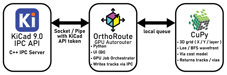
The OrthoRoute plugin communicates with KiCad via the IPC API over a UNIX-ey socket. This API is basically a bunch of C++ classes that gives me access to board data – nets, pads, copper pour geometry, airwires, and everything else. This allows me to build a second model of a PCB inside a Python script and model it however I want. With a second model of a board inside my plugin, all I have to do is draw the rest of the owl.
Development of the Manhattan Routing Engine
After wrapping my head around the the ability to read and write board information to and from KiCad, I had to figure out a way to route this stupidly complex backplane. A non-orthogonal autorouter is a good starting point, but I simply used that as an exercise to wrap my head around the KiCad IPC API. The real build is a ‘Manhattan Orthogonal Routing Engine’, the tool needed to route my mess of a backplane.
Project PathFinder
The algorithm used for this autorouter is PathFinder: a negotiation-based performance-driven router for FPGAs. My implementation of PathFinder treats the PCB as a graph: nodes are intersections on an x–y grid where vias can go, and edges are the segments between intersections where copper traces can run. Each edge and node is treated as a shared resource.
PathFinder is iterative. In the first iteration, all nets (airwires) are routed greedily, without accounting for overuse of nodes or edges. Subsequent iterations account for congestion, increasing the “cost” of overused edges and ripping up the worst offenders to re-route them. Over time, the algorithm converges to a PCB layout where no edge or node is over-subscribed by multiple nets.
With this architecture – the PathFinder algorithm on a very large graph, within the same order of magnitude of the largest FPGAs – it makes sense to run the algorithm with GPU acceleration. There are a few factors that went into this decision:
- Everyone who’s routing giant backplanes probably has a gaming PC. Or you can rent a GPU from whatever company is advertising on MUNI bus stops this month.
- The PathFinder algorithm requires hundreds of billions of calculations for every iteration, making single-core CPU computation glacially slow.
- With CUDA, I can implement a SSSP (parallel Dijkstra) to find a path through a weighted graph very fast.
Adapting FPGA Algorithms to PCBs
The original PathFinder paper was, “A Negotiation-Based Performance-Driven Router for FPGAs” and from 1995, this meant early FPGAs like the Xilinx 3000 series and others manufactured by Tryptych. These devices were simple, and to get a good idea of how they worked, check out Ken Shirriff’s blog. Here’s what the inside of a Xilinx XC2064 looks like:
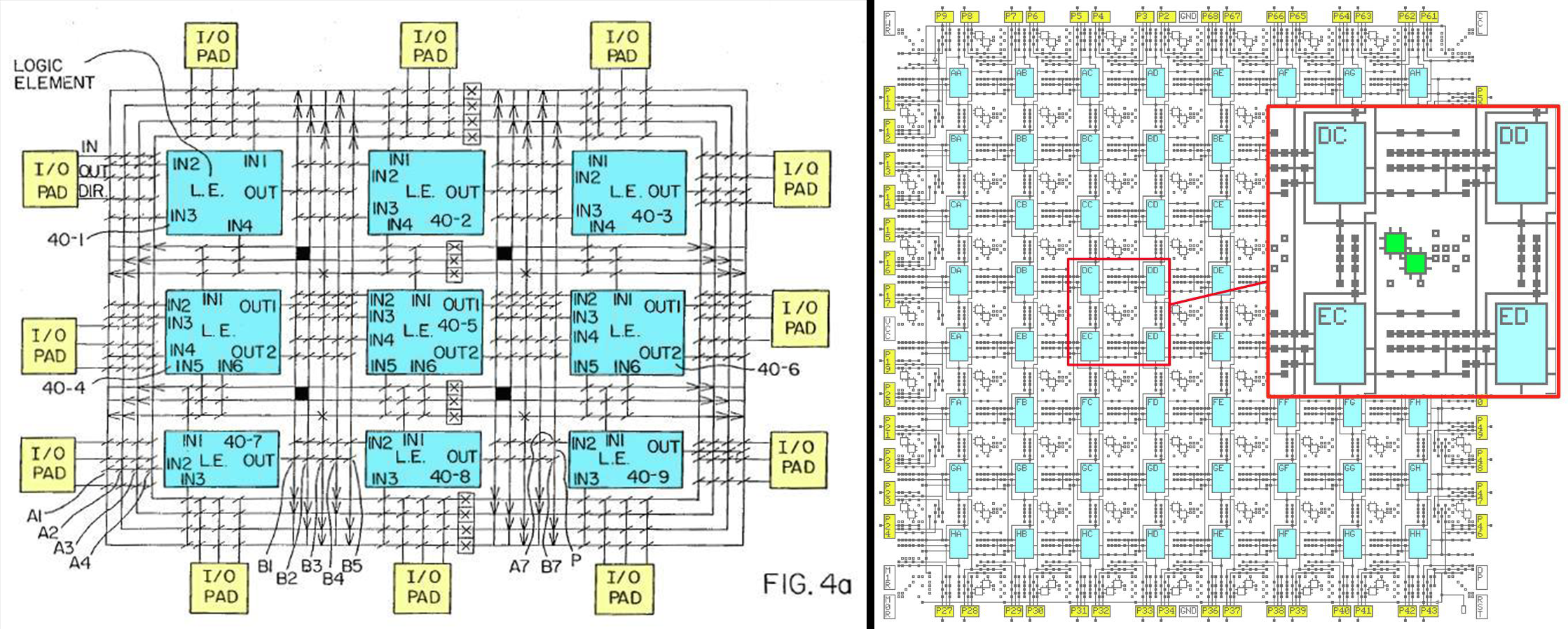
That looks complicated, but it’s really exceptionally simple. All the LUTs, or logic elements, are connected to each other with wires. Where the wires cross over, there are fuzes. Burn the fuzes and you’ve connected the wires together. It’s a simple graph and all the complexity of the actual paths inside the chip are abstracted away. For a circuit board, I don’t have this luxury. I have to figure out how to get the signal from the pads on the top layer of the PCB and ‘drill down’ with vias into the grid. I need to come up with some way to account for both the edges of the graph and nodes of the graph, something that’s untread territory with the PathFinder algorithm.
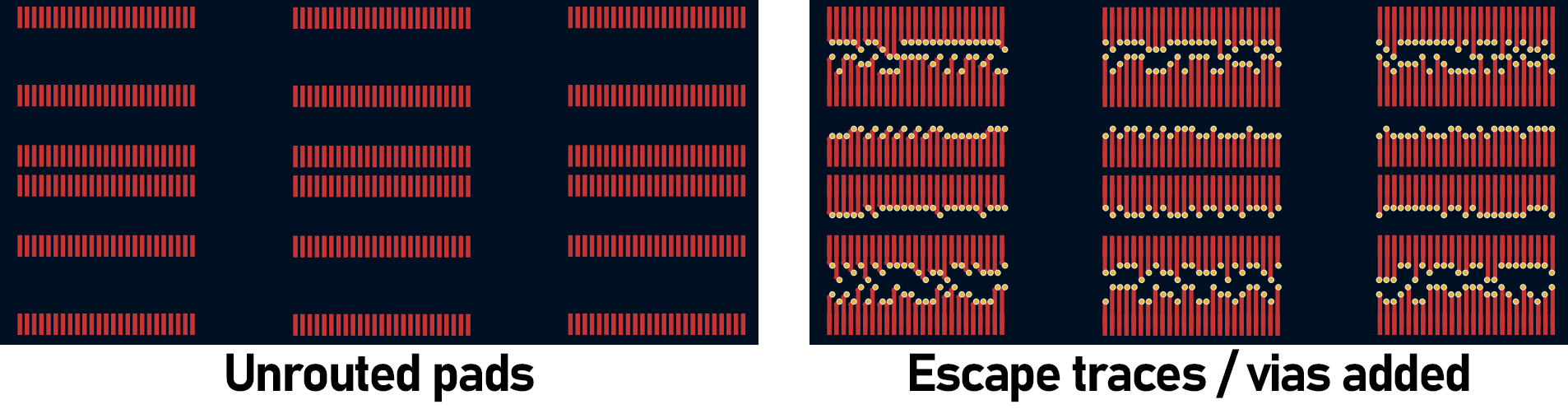
The first step of that is the pad escape planner that pre-computes the escape routing of all the pads. Because the entire Manhattan Routing Engine is designed for a backplane, we can make some assumptions: All of the components are going to be SMD, because THT parts would kill the efficiency of a routing lattice. The components are going to be arranged on a grid, and just to be nice I’d like some ‘randomization’ in where it puts the vias punching down into the grid. Here’s what the escape planning looks like:
How PathFinder Almost Killed Me, and How I made PathFinder not suck
I found every bug imaginable while developing OrthoRoute. For one, congestion of nets would grow each iterations. The router would start fine with 9,495 edges with congestion in iteration 1. Then iteration 2: 18,636 edges. Iteration 3: 36,998 edges. The overuse was growing by 3× per iteration instead of converging. Something was fundamentally broken. The culprit? History costs were decaying instead of accumulating. The algorithm needs to remember which edges were problematic in past iterations, but my implementation had history_decay=0.995, so it was forgetting 0.5% of the problem every iteration. By iteration 10, it had forgotten everything. No memory = no learning = explosion.
With the history fixed, I ran another test. I got oscillation. The algorithm would improve for 12 iterations (9,495 → 5,527, a 42% improvement!), then spike back to 11,817, then drop to 7,252, then spike to 14,000. The pattern repeated forever. The problem was “adaptive hotset sizing”—when progress slowed, the algorithm would enlarge the set of nets being rerouted from 150 to 225, causing massive disruption. Fixing the hotset at 100 nets eliminated the oscillation.
Even with fixed hotsets, late-stage oscillation returned after iteration 15. Why? The present cost factor escalates exponentially: pres_fac = 1.15^iteration. By iteration 19, present cost was 12.4× stronger than iteration 1, completely overwhelming history (which grows linearly). The solution: cap pres_fac_max=8.0 to keep history competitive throughout convergence.
PathFinder is designed for FPGAs, and each and every Xilinx XC3000 chip is the same as every other XC3000 chip. Configuring the parameters for an old Xilinx chip means every routing problem will probably converge on that particular chip. PCBs are different; every single PCB is different from every other PCB. There is no single set of history, pressure, and decay parameters that will work on every single PCB.
What I had to do was figure out these paramaters on the fly. So that’s what I did. Right now I’m using Board-adaptive parameters for the Manhattan router. Before beginning the PathFinder algorithm it analyzes the board in KiCad for the number of signal layers, how many nets will be routed, and how dense the set of nets are. It’s clunky, but it kinda works.
Where PathFinder was tuned once for each family of FPGAs, I’m auto-tuning it for the entire class of circuit boards. A huge backplane gets careful routing and an Arduino clone gets fast, aggressive routing. The hope is that both will converge – produce a valid routing solution – and maybe that works. Maybe it doesn’t. There’s still more work to do.
Routing The Monster Board
After significant testing with “small” boards (actually 500+ net subsets of my large backplane, with 18 layers), I started work on the entire purpose of this project, the 8000+ net, 17000 pad monster board. There was one significant problem: it wouldn’t fit on my GPU. Admittedly, I only have a 16GB Nvidia 5080, but even this was far too small for the big backplane.
This led me to develop a ‘cloud routing solution’. It boils down to extracting a “OrthoRoute PCB file” from the OrthoRoute plugin. From there, I rent a Linux box with a GPU and run the autorouting algorithm with a headless mode. This produces an “OrthoRoute Solution file”. I import this back into KiCad by running the OrthoRoute plugin on my local machine, and importing the solution file, then pushing that to KiCad.
Here’s the result:
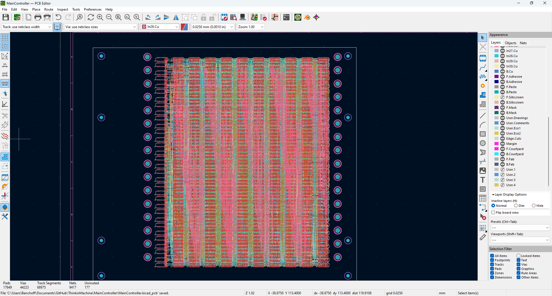
That’s it, that’s the finished board. A few specs:
- 44,233 blind and buried vias. 68,975 track segments.
- Routed on an 80GB A100 GPU, rented on vast.io. The total VRAM required to route this board was 33.5 GB, so close to being under 32GB and allowing me to rent a cheaper GPU
- Total time to route this board to completion was 41 hours. This is far better than the months it would have taken FreeRouting to route this board, but it’s still not fast.
- The routing result is good but not great. A big problem is the DRC-awareness of the escape pad planning. There are traces that don’t quite overlap, but because of the geometry generated by the escape route planner they don’t pass a strict DRC. This could be fixed in future versions. There are also some overlapping traces in what PathFinder generated. Not many, but a few.
While the output from my autorouter isn’t perfect, no one would expect an autorouter to produce a perfect result, ready for production. It’s an autorouter, something you shouldn’t trust. Turning the result for OrthoRoute into a DRC-compliant board took a few days, but it was far easier than the intractable problem of eight thousand airwires I had at the beginning.
The Future of OrthoRoute
I built this for one reason: to route my pathologically large backplane. Mission accomplished. And along the way, I accidentally built something more useful than I expected.
OrthoRoute proves that GPU-accelerated routing isn’t just theoretical, and that algorithms designed for routing FPGAs can be adapted to the more general class of circuit boards. It’s fast, too. The Manhattan lattice approach handles high-density designs that make traditional autorouters choke. And the PathFinder implementation converges in minutes on boards that would take hours or days with CPU-based approaches.
More importantly, the architecture is modular. The hard parts—KiCad IPC integration, GPU acceleration framework, DRC-aware routing space generation are done. Adding new routing strategies on top of this foundation is straightforward. Someone could implement different algorithms, optimize for specific board types, or extend it to handle flex PCBs.
The code is up on GitHub. I’m genuinely curious what other people will do with it. Want to add different routing strategies? Optimize for RF boards? Extend it to flex PCBs? PRs welcome, contributors welcome.
And yes, you should still manually route critical signals. But for dense digital boards with hundreds of mundane power and data nets? Let the GPU handle it while you grab coffee. That’s what autorouters are for.
Never trust the autorouter. But at least this one is fast.