
Recreating the Connection Machine: 4,096 RISC-V Cores in a Hypercube
I made a supercomputer out of a bunch of smartphone connectors, chips from RGB mechanical keyboards, and four thousand RISC-V microcontrollers. On paper, it has a combined clock rate over one Terahertz. The memory bandwidth is several Gigabits per second. These are real numbers, because I remember old issues of PC Gamer and their ilk doing the same thing. It’s faster than your laptop on some matrix operations, on paper. In reality, it can’t run Doom. But it will do beautiful and cursed parallel math behind a smoked acrylic panel studded with blinkenlights.
Introduction
In 1985, Thinking Machines built the Connection Machine CM-1. This was a parallel computer with 65,536 individual processors arranged at the vertexes of a 16-dimension hypercube. This means each processor in the machine is connected to 16 adjacent processors.
The Connection Machine was the fastest computer on the planet in the late 1980s (The Top500 list of supercomputers only goes back to 1993), and was purchased by various three-letter agencies, NASA, and a few well-funded universities.
Like most tech companies, Thinking Machines was a defense contractor pretending to be a cool and exciting business. When the Cold War ended, DARPA cut their funding and the company officially died in 1994. By this time, Moore’s Law had kicked in and workstations from Sun (and others) made the idea of a five million dollar machine that only spoke Lisp untenable for most companies.
Blame Gorbachev, the second AI winter, or a takedown of hypercubes as a concept in IEEE Transactions on Computers, by the mid 1990s Thinking Machines was dead. By the turn of the millenium, all of the Connection Machines were out of service. There’s one in the New York MoMA, but it’s not on display. Same with the Smithsonian. There’s one at the Computer History Museum, but the lights don’t work. The Living Computers museum had one, but it has since disappeared. The machines that remain don’t work, and there’s zero code available for these machines. So I built one.
This project is a modern recreation or reinterpretation of the lowest-spec Connection Machine built. It contains 4,096 individual RISC-V processors, each connected to 12 neighbors in a 12-dimensional hypercube. This project is heavily inspired by the work of others, and takes previous work to its logical conclusion.
Today, a ‘massively parallel computer’ means wiring up a bunch of machines running Linux to an Ethernet switch. The Connection Machine is different. In a machine with 65,536 processors, every processor is connected to 16 other processors. In my machine, there are 4,096 processors, with each one connected to 12 others. For n total processors, each node connects to exactly $\log_2(n)$ neighbors. This topology makes the machine extremely interesting with regard to what it can calculate efficiently, namely matrix operations, which is the basis of the third AI boom.
In 1986, this was the cutting edge of parallel computing and AI. In 2006, NASA would have used this machine for hypersonic computational fluid dynamics for the rocket that would put humans on the moon by the year 2020. In 2026, it’s a weird art project with a lot of LEDs.
The LED Panel
I know why you’re reading this, and why you clicked on the video, so I’m going to start off with the LED array before digging into massively parallel hypercube supercomputer. A million people will read this page, and all but a thousand will think this is the coolest part. Such is life.
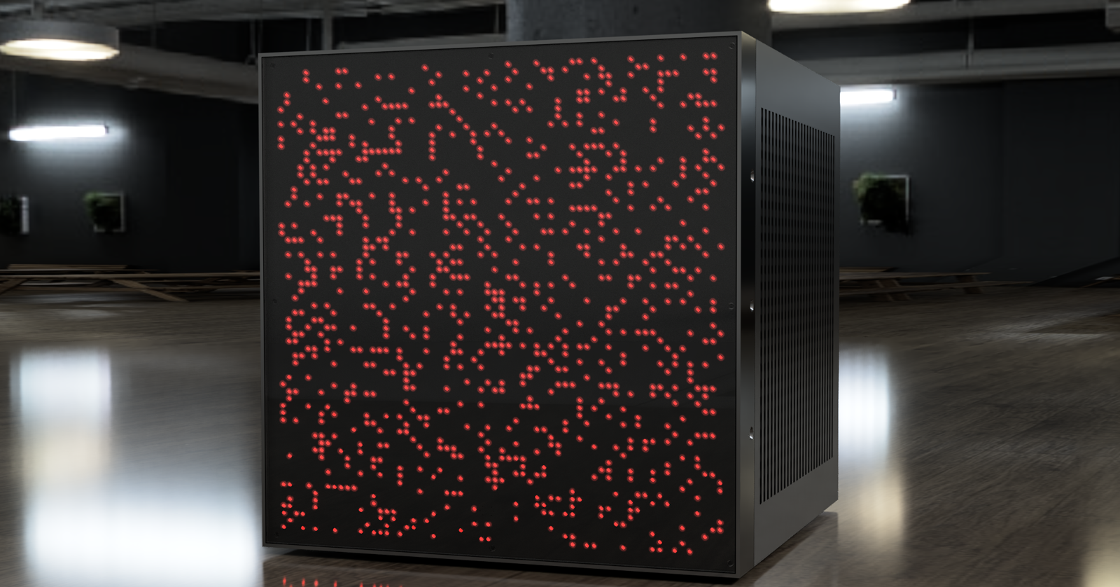
The Connection Machine was defined by a giant array of LEDs. It’s the reason there’s one of these in the MoMA, so I need 4,096 LEDs showing the state of every parallel processor in this machine. Also, blinky equals cool equals eyeballs, so there’s that.
The LED board is built around the IS31FL3741, an I2C LED matrix driver ostensibly designed for mechanical keyboard backlighting. I’ve built several projects around this chip, and have a few of these now-discontinued chips in storage.
Each IS31FL3741 is controlling an 8x32 matrix of LEDs over I2C. These chips have an I2C address pin with four possible values, allowing me to control a 32x32 array over a single I2C bus. Four of these arrays are combined onto a single PCB, along with an RP2040 (a Raspberry Pi Pico) microcontroller to run the whole thing.
LED Hardware
Why did I build my own 64x64 LED array, instead of using an off-the-shelf HUB75 LED panel? It would have certainly been cheaper – a 64x64 LED panel can be bought on Amazon for under $50. Basically, I wanted some practice with high-density design before diving into routing a 12-dimension hypercube. It’s also a quick win, giving me something to look at while routing hundreds of thousands of connections.
There are provisions to stream data from an external controller through a SPI interface at 20MHz (implemented in PIO), and through a USB connection, used mostly for testing. Data can be streamed either as black or white, or as an 8-bit grayscale. Framerate for the SPI transfer is hundreds of frames per second, although the code locks the display at 30 FPS with double buffering. This method of sending raw pixel data to the LED panel is how the 4096 cores of the machine are ultimately visualized.
Mechanically, the LED panel is a piece of FR4 screwed to the chassis of the machine. The front acrylic is Chemcast Black LED plastic sheet from TAP Plastics, secured to the PCB with magnets epoxied to the back side of the acrylic into milled slots. These magnets attach to magnets epoxied to the frame, behind the PCB. This Chemcast plastic is apparently the same material as the Adafruit Black LED Diffusion Acrylic, and it works exactly as advertised. Somehow, the Chemcast plastic turns the point source of an LED into a square at the surface of the machine. You can’t photograph it, but in person it’s spectacular.
LED Software
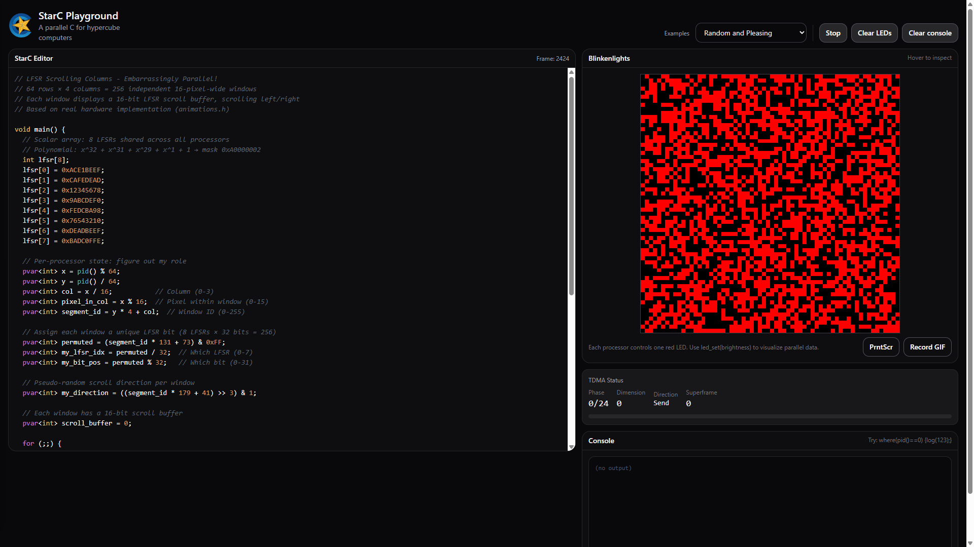
There are a few pre-programmed modes for this panel. The real showstopper is the “Random and Pleasing” mode. This is the mode shown in Jurassic Park, and it’s what MoMA turns on when they light up their machine.
There are several sources describing this mode, but only sparse details on how it’s implemented. Trammell Hudson dug into this and the basic idea is, “each processor steps through memory, and sends the bitwise OR of the memory for each processor to one LED.” That’s the CM-1. For the CM-2, it’s basically stepping through random memory. However, every single ‘reverse engineering by looking at it’ attempt implements an LFSR to generate the pixels on the grid. This is (pseudo)random, and also has the effect that the LEDs scroll left or right instead of just blinking like random static.
I went for a 4094-bit LFSR (256 taps), and divided the display up into four columns of 1x16 ‘cells’. These cells are randomly assigned to shift left or shift right, and 256 unique taps are assigned to a particular 1x16 cell. This is so much better than what you see whenever MoMA pulls their machine out of storage. It’s a digital shimmer. It’s an oil stain in a puddle in a parking lot. It’s beautiful.
Other patterns include, among others, Conway’s Game of Life, a demoscene-inspired Plasma pattern, Fire animation, and “videos” of the panel playing the first level of Doom, as well as the requisite Bad Apple animation. All of this is controlled via the RP2040 and fits on a small 2MB Flash chip. Bad Apple uses REL, the Doom screencap a weirder compression that’s best defined as bit-packing the 4-bit grayscale.
My Machine, Overview
This post has already gone on far too long without a proper explanation of what I’m building.
Very very simply, this is a very, very large cluster of very, very small computers. The Connection Machine was designed as a massively parallel computer first. The entire idea was to stuff as many computers into a box, and connect those computers together. The problem then becomes how to connect these computers. If you read Danny Hillis’ dissertation, there were several network topologies to choose from.
The nodes – the tiny processors that make up the cluster – could have been arranged as a (binary) tree, but this would have the downside of a communications bottleneck at the root of the tree. They could have been connected with a crossbar – effectively connecting every node to every other node. A full crossbar requires N², where N is the number of nodes. While this might work with ~256 nodes, it does not scale to thousands of nodes in silicon or hardware. Hashnets were also considered, where everything was connected randomly. This is too much of a mind trip to do anything useful.
The Connection Machine settled on a hypercube layout, where in a network of 8 nodes (a 3D cube), each node would be connected to 3 adjacent nodes. In a network of 16 nodes (4D, a tesseract), each node would have 4 connections. A network of 4,096 nodes would have 12 connections per node, and a network of 65,536 nodes would have 16 connections per node.
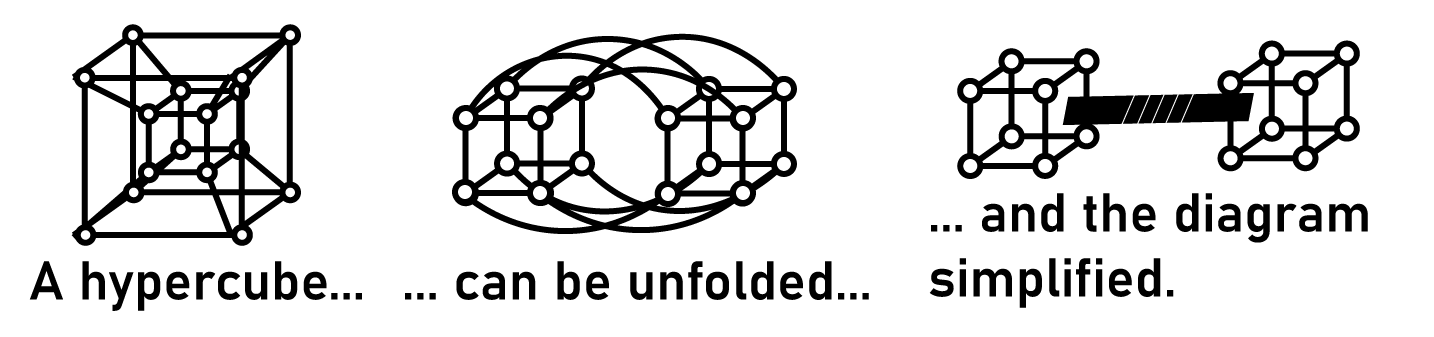
The advantages to this layout are that routing algorithms for passing messages between nodes are simple, and there are redundant paths between nodes. If you want to build a hypercluster of tiny computers, you build it as a hypercube.
Hardware Architecture
This machine is split up into segments of various sizes. Each segment is 16× bigger than the previous. These are:
- The Node This is just a small RISC-V microcontroller, controlled by another microcontroller.
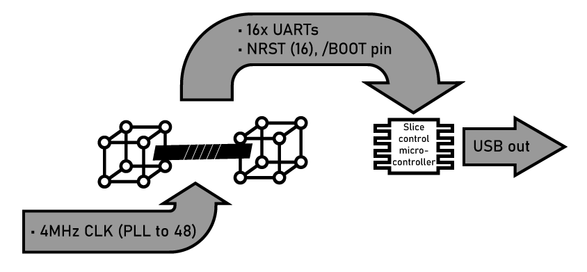
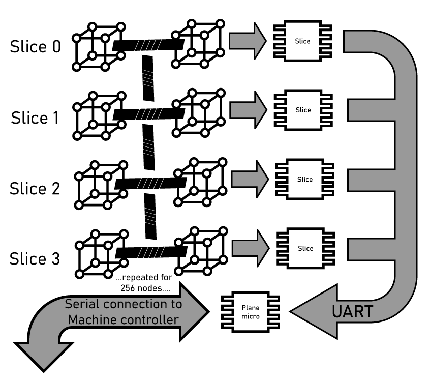
- The Slice This is 16 individual nodes, connected as a 4-dimension hypercube. In the Slice, a seventeenth microcontroller handles the initialization and control of each individual node. This means providing the means to program and read out memory from each node individually.
- The Plane 16 Slices. The Plane is 256 microcontrollers are connected as an 8-dimension hypercube. There are sixteen ‘slice controller’ microcontrollers, plus one additional ‘plane controller’. This means each plane consists of 273 individual chips.
- The Machine Sixteen Planes make a Machine. The architecture follows the growth we’ve seen up to now, with 4096 ‘node’ microcontrollers connected as a 12-dimensional hypercube. There are 4368 chips in The Machine, all controlled with a rather large SoC.
Like the original Connection Machine, there are two ‘modes’ of connection between the nodes in the array. The first is the hypercube connection, where each node connects to other nodes. The second is a tree. Each node in the machine is connected to the ‘Slice controller’ via UART. This Slice controller handles reset, boot, programming, and loading data into each node. Above the Slice is the Plane and a single ‘plane controller’ for each group of 256 nodes. And above that is the master controller.
This “hypercube and tree” is seen in other massively parallel machines of the 1980s. The Cosmic Cube at Caltech split the connections with individual links between nodes and a tree structure to a ‘master’ unit. The Intel iPSC used a similar layout, but routing subsets of the hypercube through MUXes and Ethernet, with a separate connection to a ‘cube manager’. Likewise, the Connection Machine could only function when connected to a VAX that handled the program loading and getting data out of the hypercube.
Which Microcontroller To Use
The original inspiration for this build is bitluni’s CH32V003-based Cheap RISC-V Supercluster for $2, and it would make sense to focus on something in the CH32V family. They’re cheap, they’re available on LCSC, and they’re reasonably well supported. The CH32V003 is weird though; it only has one UART interface, and the ‘hypercube and tree’ architecture really needs at least two UARTs. Programming the ‘003 chip is just slightly more difficult than I would want.
An alternative to the CH32V003 is the CH32V203. This is a faster, more capable chip based on a RISC-V4B core. It has one-cycle hardware multiply. It’s easier to program. The CH32V003 is thirteen cents in quantity, the CH32V203 is thirty-seven cents in quantity. If I’m going this far, I’ll spend the extra thousand dollars to get a machine that’s a hundred times better.
However, the CH32V203 is not the ideal choice for this machine. A key consideration to chip selection is that the second (hypercube) UART must be capable of being assigned to any pin. The CH32V203 does not have this capability; the USART1_TX can only be mapped to pins PA9 or PB6. The reason we need UART pins fully remapable are covered below, but it is a requirement for the full machine.
Most other microcontrollers have this limitation of peripherals that can only be assigned to specific pins. The PY32 series of ARM Cortex chips support up to five UARTs, but the TX and RX of these UARTs are limited to specific pairs of pins. This is a big limitation for my machine, and I wonder why fully remappable peripherals aren’t as common as I would like. Is there a patent or some shit?
There are several microcontrollers that do have fully remappable peripherals, where a UART can be attached to any pin. The NXP LPC800 series has fully remappable pins, but it’s a slightly expensive part and limited to a CPU frequency of 15MHz. The LPC800 is also an Arm Cortex-M0+ microcontroller, not a RISC-V part. This different architecture is a critical shortcoming if I want to target the Twitter, Reddit, and Hacker News crowds for this project. I gotta get eyeballs on this, after all.
The Cypress / Infineon PSOC has remappable peripherals, but these parts are even more expensive than the LPC800. The Microchip PIC32MM has a crossbar called a ‘peripheral pin select’, but it’s 2026 and I’m not using a PIC. The Raspberry Pi Pico RP2350 has PIOs, or small state machines that can assign functions to any pin. The RP2350 also has (optional) RISC-V cores, perfect for the people who appreciate tech YouTubers telling them what to think. The Pico is an expensive part, though. On paper, the RP2354A – the part with an integrated 2MB NOR Flash – could work. But having exactly as many PIOs as the number of hypercube dimensions is clunky. The Pico is right on the cusp of being workable for this machine, but not enough so that it would be easy to make it work.
There is a better option: The AG32 SoC family from AGM Micro. This family combines a RISC-V microcontroller core with a small (2000 LUT) FPGA fabric. The chip is essentially a RISC-V core, with all pins broken out to an FPGA fabric. With this, I can remap UARTS dynamically and talk to the hypercube nodes without bogging down the RISC-V core. The smallest AG32 is available for eighty cents in quantity from LCSC in a QFN32 package. This is almost the ideal chip.
The AG32 has one significant shortcoming: there is zero documentation in English. The plan is to build up as much of the machine as I can using the CH32V203. In parallel, I’ll work on getting a build system working for the AG32-series microcontrollers. Eventually, hopefully, the full machine will use thousands of these really cool RISC-V + FPGA microcontrollers.
1 Node
The goal of the 1-node prototype is to program a cheap RISC-V microcontroller with another microcontroller. This can be done with a dev/breakout board for any of the cheap RISC-V chips, so I found the WeAct Studio CH32V203C8T6. After receiving the CH32V203 dev board, I wired it up to the closest Raspberry Pi Pico-shaped object within reach:
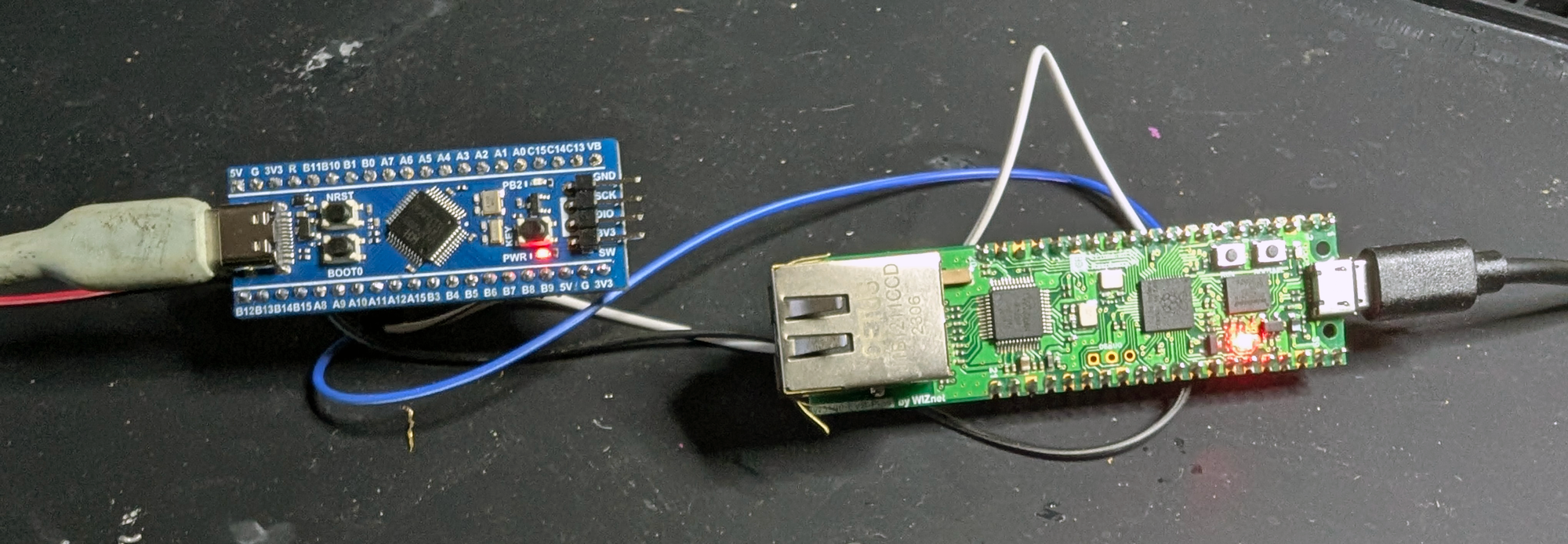
It’s just serial lines between two chips. The code is where things get fun.
The CH32V203 can be programmed over a UART presented on pins PA9 and PA10. This is easy enough to wire up, the problem comes when trying to talk to the bootloader in the CH32V203.
There’s an WCH RISC-V Microcontroller Web Serial ISP that will program these chips for you, provided you have a USB to UART converter and a firmware file for the program you want to run on this chip. For a user, the process is pretty simple, you just hold down the Boot0 pin and click upload. Underneath the hood things fall off the rails. Programming the chip works like this:
- Listen to the chip in bootloader mode - the CH32 will send data over the serial connection, and this requires a “password”, a fixed ASCII string that’s
MCU ISP & WCH.CN. The bootloader rejects everything if you don’t send that exact string. - Read the chip config - the programmer sends a bitmask to read everything, and the CH32 sends back option bytes (can the Flash memory be programmed?), the bootloader version, and an 8-byte unique ID (UID)
- Generate a Key - creates a random seed length of 30 bytes, computes a ‘seed’ with the UID and random seed, computes an 8-byte key using specific indexes from that seed and XORs it with the UID checksum. This is sent to the bootloader, and the bootloader replies with a key checksum byte, that should match what the programmer has. Why the hell it does this I have no idea. You already have physical access to the chip, what’s the threat model here?
- Erases all the flash
- Writes the new program in chunks of 56 bytes, XORed with the key
- Generates a key again
- Verifies the flash with the new key
- Resets the CH32, letting it start up with the firmware you just wrote.
Yes, this was a massive pain to figure out what was actually happening. The good news is I didn’t have to do all the work. The WCH-web-ISP code is right there, so I just told the RP2040 to do whatever the Javascript on that page was doing.
The actual payload can be anything I want. I whipped up a slightly more sophisticated ‘Hello World’ and ‘Blink a LED’ program for the CH32, compiled it, and created a firmware.h file for the Pico uploader. The contents of this .h file is just a hex dump of the .bin file built by the compiler.
After uploading the new firmware for the CH32 with a Pico, I have verification that this just might work. I can program the microcontrollers of a hypercube, so it’s time to build a hypercube.
16 Nodes, The Slice
A more complete build log for the 16 node prototype is available here
This is where the build starts getting serious. The purpose of the 16-node prototype is to verify the previous work of the 1-node build (programming via UART, external clocking) as well as defining the links between nodes, synchronization, and message passing between nodes. This is hard, and it’s a good idea to do this on a prototype board before scaling up to larger builds.
The Slice is a 4-dimensional hypercube, or 16 microcontrollers, each connected to 4 others. These 16 nodes are controlled by a dedicated microcontroller, programming each node over serial, toggling the reset circuit, and loading data into and out of each node.
The dedicated microcontroller used for this board is the RP2040. I’m using this chip for a few reasons. First, the PIOs. The PIOs in the RP2040 are small state machines that have access to GPIOs and memory via DMA that run independently of the core. I have used this functionality before to generate clock signals and read data directly into memory, as well as controlling the I2C lines in the LED panel. The PIOs are fantastic little peripherals that enable me to program a clock sent to all of the ‘Slice’ microcontrollers and read serial output. It’s a lot easier and cheaper than finding a microcontroller with 16 independent UARTs, too.
Hypercube Communication
Before digging into how nodes in my machine communicate, I’d like to outline how the nodes in the original Connection Machine communicated. Each chip (which contained several ‘nodes’) had a router, and each router had a buffer for stored messages. This enabled any node to talk to any other node, and was the most expensive part of the computer. This makes sense; the actual compute nodes were glorified ALUs. The routers were the majority of the silicon die area in the Connection Machine.
The routers were a problem. They were an engineering hassle, as it was silicon that wasn’t going to compute. Routers sucked in production. The NASA Assessment of the Connection Machine says actually using the routers for arbitrary routing is a terrible programming practice. It just made the machine slower. The way to use a Connection Machine is to only pass messages along the edges of the hypercube.
When Feynman was working on the CM-1, he analyzed the router by treating boolean circuits as a continuous, differentiable system. Hillis wrote:
Our discrete analysis said we needed seven buffers per chip; Feynman's equations suggested that we only needed five. We decided to play it safe and ignore Feynman.
The decision to ignore Feynman's analysis was made in September, but by next spring we were up against a wall. The chips that we had designed were slightly too big to manufacture and the only way to solve the problem was to cut the number of buffers per chip back to five. Since Feynman's equations claimed we could do this safely, his unconventional methods of analysis started looking better and better to us. We decided to go ahead and make the chips with the smaller number of buffers.
I looked at the same problem, thought really hard, and realized that you didn’t need routers.
CSMA vs TDMA
To actually pass messages back and forth between nodes through the hypercube array, we need a way to arbitrate the connections – which node actually gets to use the connection at any point in time. There are several ways to do this.
CSMA:
The naive way to arbitrate message passing between nodes is carrier-sense multiple access, or CSMA. Consider two nodes. At rest, the line is pulled high, because of a pullup. For node Alice to talk to node Bob, Alice first pulls the line low for some number of microseconds. Bob detects the line is low, and starts listening. Then Alice starts sending data. If Bob wants to talk to Alice, Bob pulls the line low, waits, then sends data. Alice listens.
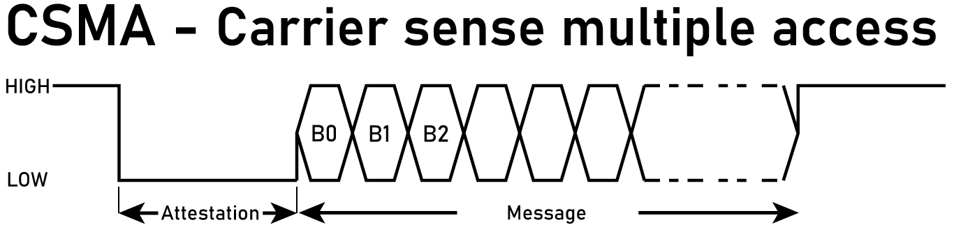
This has significant drawbacks. There will be collisions, where both nodes want to talk at the same time. I would have to add backoff timers and retries, and god forbid acknowledgements. The code to do this is gnarly, and I simply don’t want to do it. Because there’s a better way.
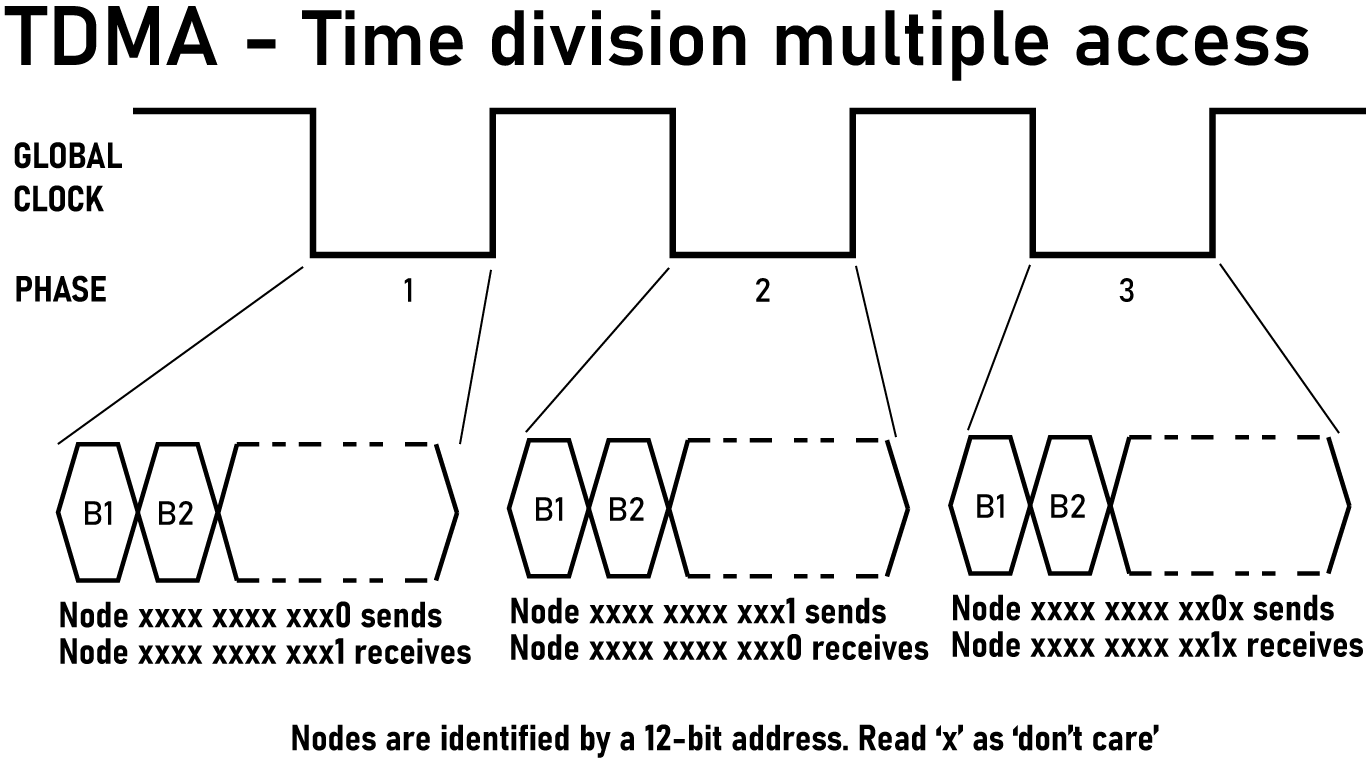
TDMA:
A more thorough explanation of the TDMA messaging scheme is available here
Consider the actual topology of what’s communicating here. All nodes are assigned a 12-bit number. Each connection is to a processor that is a single bit flip away. Node 0x2A3 is connected to node 0x2A2 (bit 0 flipped), node 0x2A1 (bit 1 flipped), node 0x2AB (bit 3 flipped), and so on.
Now define a global tick counter, synchronized across all nodes via the shared clock from the slice controllers. The phase is just tick mod 24 - twelve dimensions, two directions each. In phase d, only dimension d links are active. All other links stay idle. Within that phase, the node with addr[d] == 0 transmits first, then the node with addr[d] == 1 transmits in the second half. This is time-division multiple access, or TDMA.
Or, if you prefer text form:
- Phase 0: Nodes with address
xxxx xxxx xxx0sends → Nodesxxxx xxxx xxx1receives - Phase 1: Nodes with address
xxxx xxxx xxx1sends → Nodesxxxx xxxx xxx0receives - Phase 2: Nodes with address
xxxx xxxx xx0xsends → Nodesxxxx xxxx xx1xreceives - Phase 3: Nodes with address
xxxx xxxx xx1xsends → Nodesxxxx xxxx xx0xreceives - Phase 4: Nodes with address
xxxx xxxx x0xxsends → Nodesxxxx xxxx x1xxreceives - Phase 5: Nodes with address
xxxx xxxx x1xxsends → Nodesxxxx xxxx x0xxreceives - And so on for 24 phases…
The brilliant part about this is that no node ever talks to its neighbor at the same time. Collisions are impossible, and this scheme vastly simplifies the UART code for each node. In fact, because only dimension connection is active at any one time, I ONLY NEED ONE UART FOR THE HYPERCUBE, reconfigured for different pins for each phase.
Since only one dimension is active per phase, each node only needs to speak on one physical link at a time. If the UART can be remapped fast enough, one hardware UART can time-multiplex across all 12 links. The hypercube unfolds into time. Twelve dimensions become twenty-four phases, and the topology is temporal as much as spatial. Now we have a counter to the redditor who will say, “well acktually it’s not a true hypercube because we live in four dimensions, three spacial dimension plus time.” We can now tell that loser to stuff it.
It’s also fast:
Throughput at various baud rates:
| Baud Rate | Per-Link BW | Per-Node BW | Machine Aggregate |
|---|---|---|---|
| 115.2 kbps | 4.8 kbps | 115.2 kbps | 236 Mbps |
| 500 kbps | 20.8 kbps | 500 kbps | 1.02 Gbps |
| 1 Mbps | 41.7 kbps | 1 Mbps | 2.05 Gbps |
| 2 Mbps | 83.3 kbps | 2 Mbps | 4.1 Gbps |
Latency at various phase rates:
| Phase Rate | Phase Duration | Bits per Phase @ 1Mbps | 12-Hop Latency |
|---|---|---|---|
| 1 kHz | 1 ms | 1000 bits | 144 ms |
| 10 kHz | 100 µs | 100 bits | 14.4 ms |
| 100 kHz | 10 µs | 10 bits | 1.44 ms |
| 1 MHz | 1 µs | 1 bit | 144 µs |
There’s a catch with this plan
As discussed above, most chips, including the CH32V203, can not assign UART functions to any pin. The CH32V203 does not have this pin remapping function. The AG32VF-ASIC from AGM Micro can do this. This chip is a RISC-V RV32IMAFC microcontroller bolted onto a CPLD with 2K LUTs. All peripheral functions can be mapped onto any pin, and this can be done dynamically. It’s eighty cents a piece on LCSC.
This is actually going to work And with TDMA, 16-node prototype verifies everything needed for the full 4096-node machine. If TDMA works with 16 nodes, it’ll work with 4096.
I want to take a step back here and just point out I’m designing a machine that can move a gigabit or more per second around its memory, does this with a single hardware UART, and is built out of thirty cent RISC-V microcontrollers. All of this just falls out of the topology of the machine. Instead of a furball of code trying to get rid of problems with carrier sense, TDMA based on the address of the node solves the problem elegantly.
This should be your first realization that the hypercube architecture is recursively elegant. If you construct a parallel computer with a hypercube architecture, cool stuff just appears.
Two documents were created to explain the 16 node prototype, linked here:
Related pages:
256 Nodes, The Plane
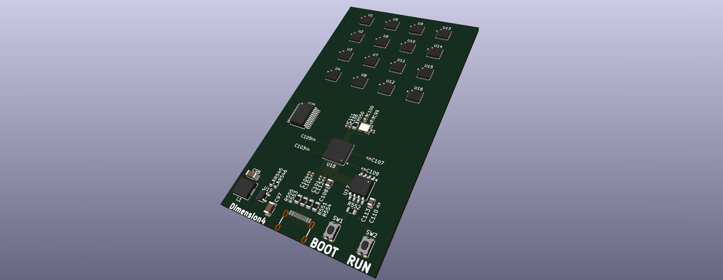
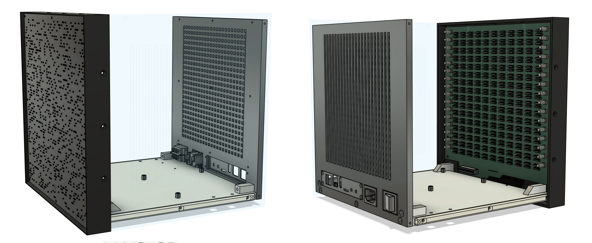
The 256 node prototype builds on the progress made with the 1-node and 16-node boards. It is effectively sixteen copies of the 16-node board, with an additional Plane controller chip talking to each of the 16 Slice controllers. This prototype is effectively also the first ‘production’ circuit; in the full machine, I’m splitting up 4096 nodes over 16 individual boards of 256 nodes. This means the 256 node prototype is also the first revision of the main processor boards that will go into the machine.
The 256 node board is also the first one prototype where things get really hairy and interesting. Each chip is connected to eight other chips in the hypercube array. For 256 chips, this means there are 2048 inter-node links. If the chips can handle this, they’re probably good for the entire 4096-node full machine.
4096 Nodes
This is where the magic happens. The original CM-1 was controlled via a DEC VAX or Lisp machine that acted as a front-end processor. The front-end would broadcast instructions to the array, collect results, and handle I/O with the outside world. My machine needs something similar. At the top of the hierarchy sits a Zynq SoC - an FPGA with ARM cores bolted on. This is the easiest way to get
This handles:
- Instruction broadcast: In SIMD mode, the Zynq sends opcodes down the tree to all 4,096 nodes simultaneously
- Result aggregation: Data flows up through the Planes, gets collected, and presents to the outside world
- Network interface: Ethernet to everything else, USB, and HDMI simply because the Zynq support it. It’s a Linux machine, after all.
- LED coordination: Someone has to tell that 64x64 array what to display
The Zynq talks to 16 Plane controllers. Each Plane controller talks to 16 Slice controllers. Each Slice controller talks to 16 nodes. It’s trees all the way down.
The Backplane
The backplane is the key to the entire machine. This is historically true for big, old machines. I’ve been inside a PDP Straight-8, and the entire computer is composed of small cards containing just a few circuits. Plug them into the backplane – a gigantic wire-wrapped monstrosity – and the computer appears out of these simple single-circuit cards. The Cray Couch, despite vastly more complicated modules, appears when you add miles of wire in between these modules. This machine is no exception.
The modular nature of my machine means I only have to design one processor board and manufacture it 16 times. Each board handles 2,048 internal connections between its 256 chips, and exposes 1,024 connections to the backplane. The backplane does all the heavy lifting. It’s where the real routing complexity lives, implementing the inter-board connections that make 16 separate 8D cubes behave like one unified 12D hypercube. The boards are segmented like this:
Board-to-Board Connection Matrix
Rows = Source Board, Columns = Destination Board, Values = Number of connections
| Board | B00 | B01 | B02 | B03 | B04 | B05 | B06 | B07 | B08 | B09 | B10 | B11 | B12 | B13 | B14 | B15 |
|---|---|---|---|---|---|---|---|---|---|---|---|---|---|---|---|---|
| B00 | 0 | 256 | 256 | 0 | 256 | 0 | 0 | 0 | 256 | 0 | 0 | 0 | 0 | 0 | 0 | 0 |
| B01 | 256 | 0 | 0 | 256 | 0 | 256 | 0 | 0 | 0 | 256 | 0 | 0 | 0 | 0 | 0 | 0 |
| B02 | 256 | 0 | 0 | 256 | 0 | 0 | 256 | 0 | 0 | 0 | 256 | 0 | 0 | 0 | 0 | 0 |
| B03 | 0 | 256 | 256 | 0 | 0 | 0 | 0 | 256 | 0 | 0 | 0 | 256 | 0 | 0 | 0 | 0 |
| B04 | 256 | 0 | 0 | 0 | 0 | 256 | 256 | 0 | 0 | 0 | 0 | 0 | 256 | 0 | 0 | 0 |
| B05 | 0 | 256 | 0 | 0 | 256 | 0 | 0 | 256 | 0 | 0 | 0 | 0 | 0 | 256 | 0 | 0 |
| B06 | 0 | 0 | 256 | 0 | 256 | 0 | 0 | 256 | 0 | 0 | 0 | 0 | 0 | 0 | 256 | 0 |
| B07 | 0 | 0 | 0 | 256 | 0 | 256 | 256 | 0 | 0 | 0 | 0 | 0 | 0 | 0 | 0 | 256 |
| B08 | 256 | 0 | 0 | 0 | 0 | 0 | 0 | 0 | 0 | 256 | 256 | 0 | 256 | 0 | 0 | 0 |
| B09 | 0 | 256 | 0 | 0 | 0 | 0 | 0 | 0 | 256 | 0 | 0 | 256 | 0 | 256 | 0 | 0 |
| B10 | 0 | 0 | 256 | 0 | 0 | 0 | 0 | 0 | 256 | 0 | 0 | 256 | 0 | 0 | 256 | 0 |
| B11 | 0 | 0 | 0 | 256 | 0 | 0 | 0 | 0 | 0 | 256 | 256 | 0 | 0 | 0 | 0 | 256 |
| B12 | 0 | 0 | 0 | 0 | 256 | 0 | 0 | 0 | 256 | 0 | 0 | 0 | 0 | 256 | 256 | 0 |
| B13 | 0 | 0 | 0 | 0 | 0 | 256 | 0 | 0 | 0 | 256 | 0 | 0 | 256 | 0 | 0 | 256 |
| B14 | 0 | 0 | 0 | 0 | 0 | 0 | 256 | 0 | 0 | 0 | 256 | 0 | 256 | 0 | 0 | 256 |
| B15 | 0 | 0 | 0 | 0 | 0 | 0 | 0 | 256 | 0 | 0 | 0 | 256 | 0 | 256 | 256 | 0 |
The Backplane Connectors
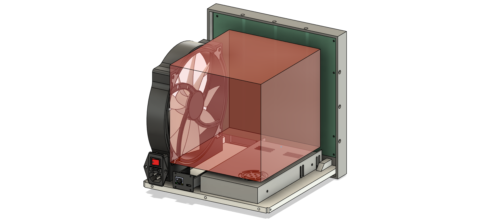
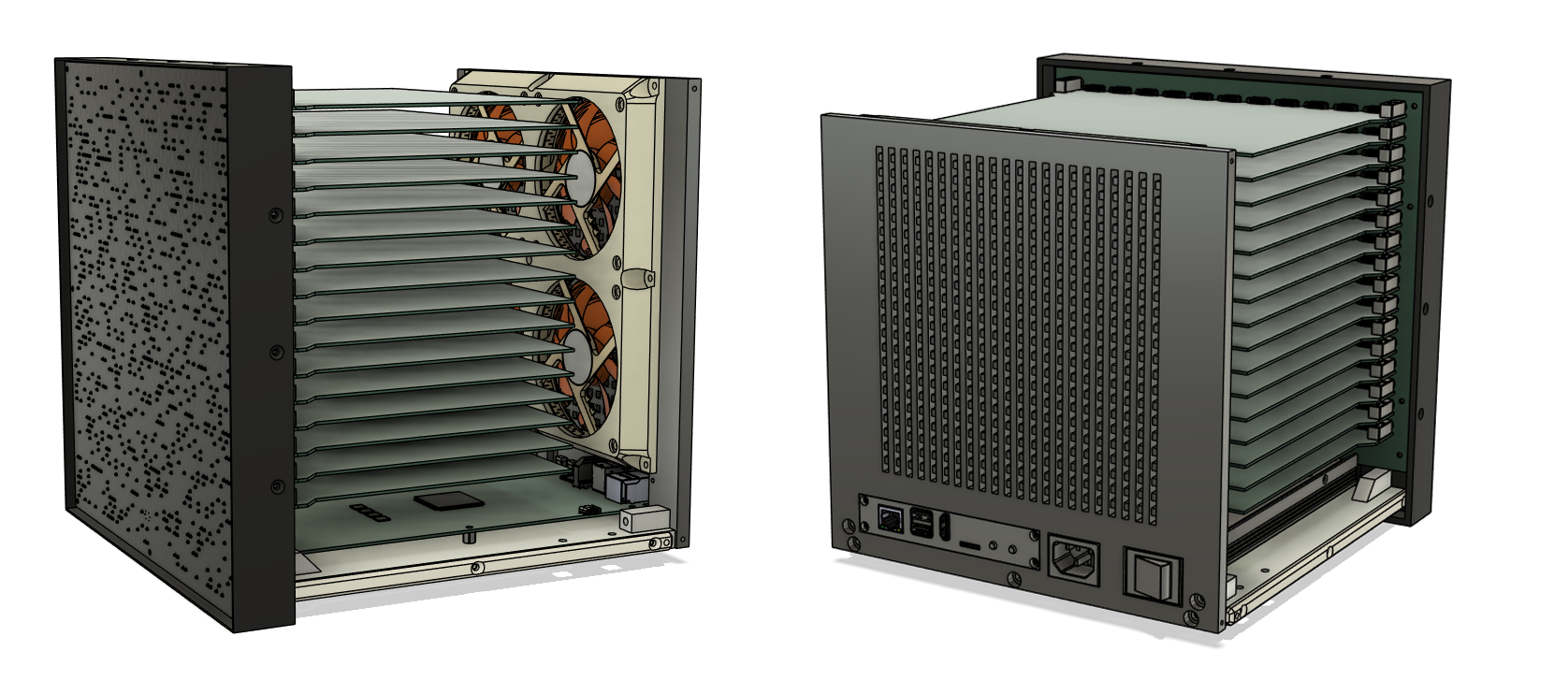
Mechanically, this device is tight. The LED panel is screwed into a frame that also holds the back plane on the opposite side. The back side has USB-C and Ethernet connections to the outside world. Internally, there’s a bunch of crap. A Mean Well power supply provides the box with 12V power. Since 4096 RISC-V chips will draw hundreds of Watts, cooling is also a necessity. A quartet of fans are bolted to the back panel of the device. Noctua on that thang.
There’s a lot of stuff in this box, and not a lot of places to put 16 boards. Here’s a graphic showing the internals of the device, with the area for the RISC-V boards highlighted in pink:
There isn’t much space to put the connectors for sixteen boards, especially connectors with 1100 pins. Dividing 1100 pins by the available length of 200mm gives us a pin pitch of 0.2mm. The pins for the connectors would have to be 0.2mm apart. This just doesn’t exist.
So how do you physically connect 1024 signals per board, in 200mm, with 10mm of height to work with? You don’t, because the connector you need doesn’t exist. After an evening spent crawling Samtec, Amphenol, Hirose, and Molex catalogs, I landed on this solution:
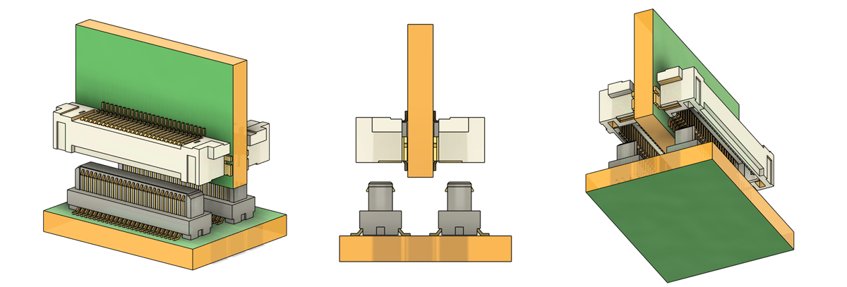
For the card-to-backplane connections, I’m using Molex SlimStack connectors, 0.4mm pitch, dual row, with 50 circuits per connector. They are Part Number 5033765020 for the right angle connectors on each card, and Part Number 545525010 for the connectors on the backplane. Instead of using a single connector on one side of the cards, I’m doubling it up, with connectors on both the top and the bottom. Effectively, I’m creating my own 4-row right angle SMT connector. Obviously, the connectors are also doubled on the backplane. This gives me 100 circuits in just 15mm of width along the ‘active’ edge of each card, and a card ‘pitch’ of 8mm. This is well within the requirements of this project. It’s insane, but everything about this project is.
With an array of 22 connectors per card – 11 on both top and bottom – I have 1100 electrical connections between the cards and backplane, enough for the 1024 hypercube connections, and enough left over for power, ground, and some sparse signalling. That’s the electrical connections sorted, but there’s still a slight mechanical issue. For interfacing and mating with the backplane, I’ll be using Samtec’s GPSK guide post sockets and GPPK guide posts. With that, I’ve effectively solved making the biggest backplane any one person has ever produced.
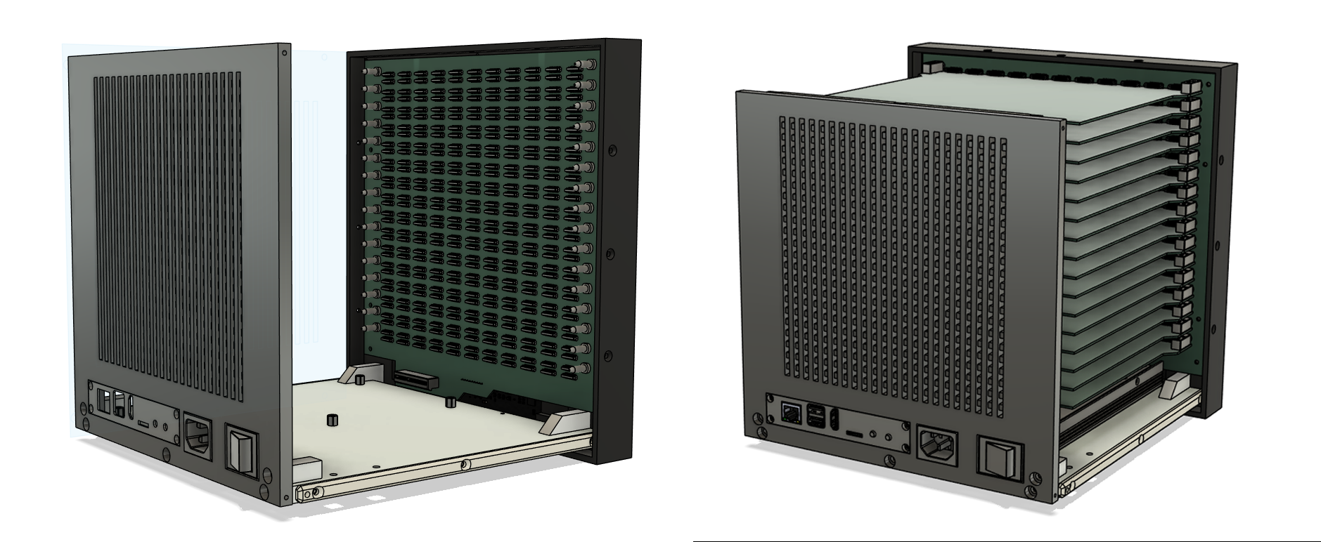
Above is a render of the machine showing the scale and density of what’s going on. Most of the front of the computer is the backplane, with the ‘compute cards’ – sixteen of the 8-dimensional hypercube boards – filling all the space. The cards, conveniently, are on a half-inch pitch, or 0.5 inches from card to card.
It’s tight, but it’s possible. The rest is only a routing problem.
OrthoRoute
This is OrthoRoute, a GPU-accelerated autorouter for KiCad. There’s very little that’s actually new here; I’m just leafing through some of the VLSI books in my basement and stealing some ideas that look like they might work. If you throw enough compute at a problem, you might get something that works.
OrthoRoute is written for the new IPC plugin system for KiCad 9.0. This has several advantages over the old SWIG-based plugin system. IPC allows me to run code outside of KiCad’s Python environment. That’s important, since I’ll be using CuPy for CUDA acceleration and Qt to make the plugin look good. The basic structure of the OrthoRoute plugin looks something like this:
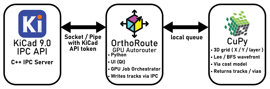
The OrthoRoute plugin communicates with KiCad via the IPC API over a Unix socket. This API is basically a bunch of C++ classes that gives me access to board data – nets, pads, copper pour geometry, airwires, and everything else. This allows me to build a second model of a PCB inside a Python script and model it however I want.
From there, OrthoRoute reads the airwires and nets and figures out what pads are connected together. This is the basis of any autorouter. OrthoRoute then uses CuPy and interesting algorithms ripped from the world of FPGA routing to turn a mess of airwires into a routed board.
The algorithm used for this autorouter is PathFinder: a negotiation-based performance-driven router for FPGAs. My implementation of PathFinder treats the PCB as a graph: nodes are intersections on an x–y grid where vias can go, and edges are the segments between intersections where copper traces can run. Each edge and node is treated as a shared resource.
PathFinder is iterative. In the first iteration, all nets (airwires) are routed greedily, without accounting for overuse of nodes or edges. Subsequent iterations account for congestion, increasing the “cost” of overused edges and ripping up the worst offenders to re-route them. Over time, the algorithm converges to a PCB layout where no edge or node is over-subscribed by multiple nets.
With this architecture – the PathFinder algorithm on a very large graph, within the same order of magnitude of the largest FPGAs – it makes sense to run the algorithm with GPU acceleration. There are a few factors that went into this decision:
- Everyone who’s routing giant backplanes probably has a gaming PC. Or you can rent a GPU from whatever company is advertising on MUNI bus stops this month.
- The PathFinder algorithm requires hundreds of billions of calculations for every iteration, making single-core CPU computation glacially slow.
- With CUDA, I can implement a SSSP (parallel Dijkstra) to find a path through a weighted graph very fast.
Note this is not a fully parallel autorouter; in OrthoRoute, nets are still routed in sequence on a shared congestion map. The parallelism lives inside the shortest-path search: a CUDA SSSP (“parallel Dijkstra”) kernel makes each individual net’s pathfinding fast, but it doesn’t route many nets simultaneously.
This yak is fuckin bald now. But I think the screencaps speak for themselves:
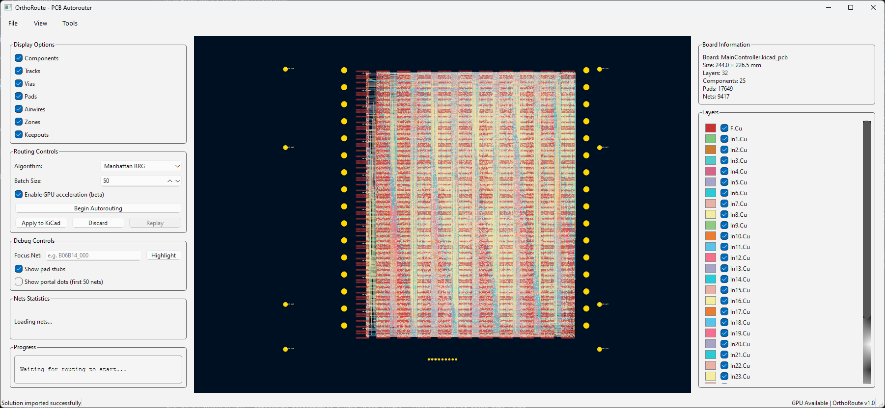
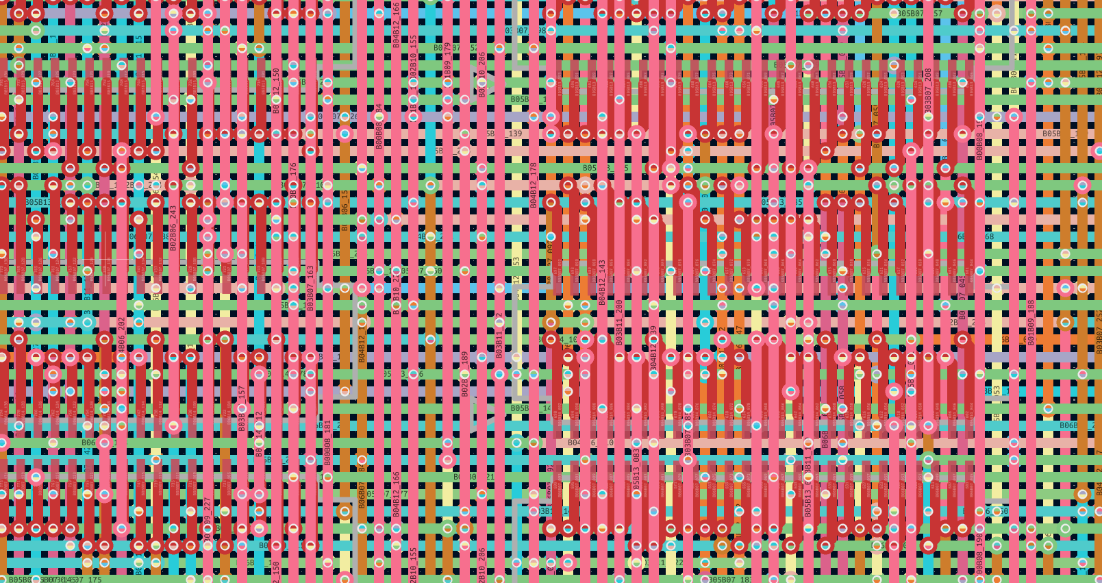
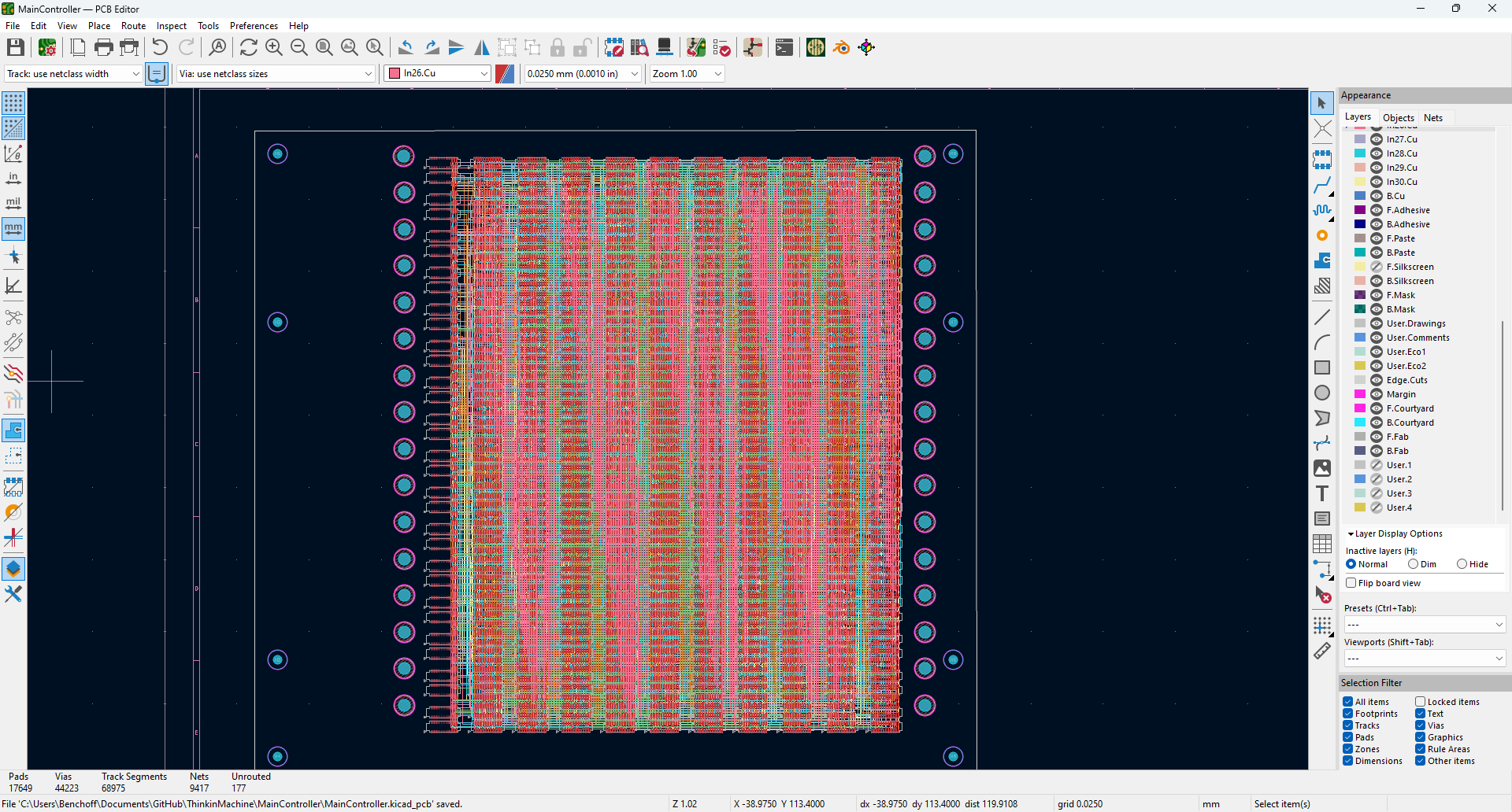
This board feels pain. You get mental damage from just looking at it. Every other board you’ve ever seen comes with the assumption that a human played some part in it. This does not; it’s purely an algorithm grinding away. It’s the worst board that you’ve ever seen.
You can run OrthoRoute yourself by downloading it from the repo. Install the .zip file via the package manager. A somewhat beefy Nvidia GPU is highly suggested but not required; there’s CPU fallback. If you want a deeper dive on how I built OrthoRoute, there’s also a page in my portfolio about it.
The Controller Board
The Connection Machine was the fastest computer on the planet, but it was also just a coprocessor. There was no video out, general purpose serial ports, or anything to connect the Connection Machine to the outside world, save for a connection to a VAX or a Symbolics Lisp machine. The front end of the Connection Machine was just a computer, so I need to design my own computer.
You might think that I would just connect a Raspberry Pi to the backplane, or build a PCB with an Allwinner chip or something. This will not work, because the backplane requires sixteen high-speed serial links to each card. The main controller will need to generate TDMA timing signals. This is not a job for a normal ARM chip running Linux, but it’s also not a job for an FPGA; this machine needs to run Linux, with Ethernet and a whole bunch of ports. So I need both an FPGA and a chip that runs Linux.
[PICTURE OF BOARD]
This is a job for an AMD/Xilinx Zynq UltraScale+ processor. It’s a System on Chip with a dual-core ARM Cortex-A53, two additional ARM Cortex-R5 cores for real-time processing, and an FPGA bolted to the silicon. The specs for the complete board are:
| Subsystem | Specification |
|---|---|
| CPU | Dual-core ARM Cortex-A53 @ 1.5 GHz + Dual Cortex-R5F real-time cores |
| GPU | Mali-400 MP2 |
| FPGA Fabric | 47,000 LUTs (Zynq UltraScale+ ZU2EG) |
| System Memory | 4 GB DDR4-2400, 32-bit bus (2× Micron MT40A1G16TB-062E) |
| Storage | 1 TB M.2 NVMe over PCIe Gen2 ×1 (~500 MB/s), via PS-GTR Lane 2 |
| Ethernet | Gigabit, Realtek RTL8211EG PHY, RGMII to Zynq GEM3 |
| USB | 4× USB 3.0 (5 Gbps), TI TUSB8043A 4-port hub, Microchip USB3300 ULPI PHY |
| Display | DisplayPort 1.2, 2-lane. Up to 4K@30Hz or 1080p@60Hz |
| Audio | TI PCM5102A I2S DAC → 3.5mm TRS jack (headphones) or Diodes PAM8302A 2.5W Class-D amp (internal speaker). |
| Backplane Interface | 16 independent UART channels + TDMA sync + LED SPI, all in FPGA fabric. |
The Internet is going to compare this to a Raspberry Pi, so let me preempt that: on paper, it’s kinda like a Raspberry Pi 3, with the Cortex-A53 running at 1.5GHz. In reality, the DDR4 is a vast improvement over the Pi3’s LPDDR2. There’s actual NVMe storage on this thing, USB3 and Gigabit Ethernet. The ‘desktop feel’ and vibe is much faster than the decade-old Raspberry Pi 3.
Exploiting Real Time Cores
Using a combination FPGA/ARM chip makes perfect sense for this application. The FPGA can instantiate all the serial transceivers I need for the hypercube tree, and it can generate the TDMA signals. The chip I’m using has a few more interesting features, like the dual Cortex-R5 cores. These are real-time processors that control the hypercube hardware directly. The R5 cluster drives all 16 backplane UARTs, generates the TDMA timing clock, controls the LED panel, and manages the fans. Linux talks to the R5 over a mailbox interface, but never touches the hypercube hardware.
Because all the peripherals on this controller board go through pins accessible to the FPGA, the R5 cores, and the Cortex-A53, I can do some really cool stuff. I dropped an I2S audio chip on the board, just so Linux could have audio. But the R5 cores also have access to the I2S lines, meaning I can have a ‘boot chime’ that plays instantly after I flip the power switch before Linux even boots. It’s just like an old Mac or a Sun workstation.
The DisplayPort is also accessible from the R5 cores, which means I can display a Linux desktop and data from the hypercube simultaneously. The DisplayPort DMA engine has a few registers that set the display width and memory stride independently. This means Linux can render 1440 pixels of a 1920-pixel framebuffer, and the R5 cores own the remaining 480 pixels. The result is a 4:3 Linux desktop on the left side of a 16:9 monitor, with a live operator console on the right showing live updates from the hypercube. It’s the coolest thing you’ve ever seen:
[SCREENCAP OF STRIDE CONTROLLER OPERATOR SCREEN HERE]
The R5 cluster also functions as a Baseboard Management Controller. Because the R5 cores operate in a separate power domain from the A53, a Linux kernel panic doesn’t affect the hypercube. I can SSH into the BMC over Ethernet, restart Linux, and the hypercube never notices. You simply couldn’t do that with a Raspberry Pi.
All the documentation for the Controller Board is available on the relevant project page.
Mechanical Design
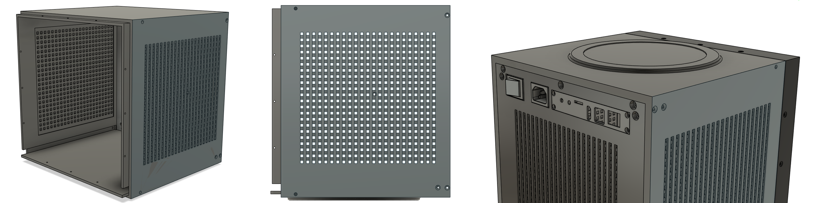
The entire thing is made out of machined aluminum plate. The largest and most complex single piece is the front – this holds the LED array, diffuser, and backplane. It attaches to the outer enclosure on all four sides with twelve screws. Attached to the front frame is the ‘base plate’ and the back side of the machine, forming one U-shaped enclosure. On the sides of the base plate are Delrin runners which slide into rabbets in the outer enclosure. This forms the machine’s chassis. This chassis slides into the outer enclosure.
The outer enclosure is composed of four aluminum plates, open on the front and back. The top panel is just a plate, and the bottom panel has a circular plinth to slightly levitate the entire machine a few millimeters above the surface it’s sitting on. The left and right panels have a grid pattern machined into them that is reminiscent of the original Connection Machine. These panels are made of 8mm plate, and were first screwed together, welded, then the screw holes plug welded. Finally, the enclosure was bead blasted and anodized matte black.
There is a small error in the grid pattern of one of the side pieces. Where most of the grid is 4mm squares, there is one opening that is irregular, offset by a few millimeters up and to the right. Somebody influential in the building of the Connection Machine once looked at the Yomeimon gate at Nikkō, noting that of all the figures carved in the gate, there was one tiny figure carved upside-down. The local mythology around this says it was done this way, ‘so the gods would not be jealous of the perfection of man’.
While my machine is really good, and even my guilt-addled upbringing doesn’t prevent me from taking some pride in it, I have to point out that I didn’t add this flaw to keep gods from being offended. I know this is not perfect. There is documentation on the original Connection Machine that I would have loved to reference, and there are implementations I would have loved to explore were time, space, and money not a consideration. The purposeful and obvious defect in my machine is simply saying that I know it’s not perfect. And this isn’t a one-to-one clone of the Connection Machine, anyway. It’s a little wabi-sabi saying forty years and Moore’s Law result in something that’s different, even if the influence is obvious.
Software Architecture
After building the hardware, with LED panels wrapped in Chemcast acrylic, plug welded aluminum frame, and a backplane that actually feels pain, you may wonder what this machine actually does. That’s a fair question. It’s elegant, beautiful, but it doesn’t really do anything useful. For many of us, that was an ex in our 20s. Now it’s a computer.
This machine is fundamentally incompatable with any programming language. The only way I have to program the 4,096 chips in the machine is through C, because that’s the toolchain I have. The real Connection Machine had a variety of languages like *Lisp, a parallel verison of Lisp, and C*, a parallel version of C. These languages don’t exist any more, insofar as I can find actual code. I can, however, look at sources and figure out how they were programmed in these languages.
C* and *Lisp and the parallel Fortran mentioned in an old NASA Ames publication all share the same basic ideas. The Connection Machine used parallel variables, where there’s one value per processor, scalar variables, which are the same value repeated on all the processors, and communication primitives like neighbor exchange, reduction, and broadcast. The languages are data-parallel, not message passing.
The problem is, there’s no existing language that does this. I can contort the C-based toolchain available for any microcontroller to do all this, but this is the sort of thing that should really be its own language, if only for error and type checking.
So I guess I have to create my own language for this computer.
StarC - Parallel C
![]()
This is StarC. It’s the language I had to write to make this machine programmable. There are three basic ideas that I’m adding to C:
Parallel variables. pvar<int> x means “every processor has its own x.” When you write x = x + 1, all 4,096 processors increment their local copy simultaneously.
Masked execution. where (x > 0) { ... } means “only processors where the condition is true execute this block.” The others skip it. This is how you express “some processors do this, others don’t” without breaking the single-program model.
Communication blocks. exchange { n = nbr(0, x); } means “every processor swaps its x with its dimension-0 neighbor.” All communication—neighbor exchange, grid neighbors, reductions, scans—happens inside exchange blocks. The runtime schedules it onto the TDMA phases. You declare what you need; the machine figures out when.
Here’s what StarC looks like in practice—a simple program that lights up processors based on their neighbors:
void main() {
    pvar alive = (pid() % 7 == 0) ? 1 : 0;  // Seed some processors
    pvar neighbor;

    for (int i = 0; i < 100; i++) {
        exchange {
            neighbor = nbr(0, alive);  // Get dimension-0 neighbor's state
        }

        where (alive == 0 && neighbor == 1) {
            alive = 1;  // Dead processors with live neighbors come alive
        }

        led_set(alive * 255);
        barrier();
    }
}
Every processor runs this same code. Each has its own alive and neighbor. The exchange block swaps values with neighbors; the where block filters which processors update. The LED panel shows the result—a pattern spreading across the hypercube, one dimension at a time.
StarC Design
StarC is deliberately minimal. The language adds exactly three constructs to C: parallel variables, masked execution, and exchange blocks. StarC is a way to make illegal programs unrepresentable on a TDMA-scheduled hypercube. That’s what the hardware requires, and what C doesn’t natively provide. Everything else is still C.
Because we’re using a TDMA schedule to program this thing, costs should be visible. This is why exchange blocks exist as explicit syntax. The hardware batches all communication into TDMA phases—you can’t scatter nbr() calls throughout your code like function calls. Making exchange blocks syntactically distinct forces you to think about communication as a discrete step: compute, exchange, compute, exchange. The code structure mirrors the hardware’s rhythm.
The where/if distinction exists for the same reason. if with a scalar condition means all processors take the same branch. where with a parallel condition means processors diverge. Exchange blocks inside where are illegal; if half the processors skip an exchange, the TDMA schedule breaks. The preprocessor catches this at compile time rather than letting it fail mysteriously at runtime.
What StarC doesn’t have is equally deliberate. There’s no send(dest, msg) even though the TDMA scheme could support multi-hop routing. The interesting hypercube algorithms—bitonic sort, parallel prefix, stencils—don’t need it. Adding arbitrary routing would invite people to write programs the hardware executes poorly. StarC restricts you to what the hypercube does well.
You might be asking yourself, “wait, I’m smart and attractive and eminently capable and wealthy, why can’t I just implement these with macros?” You could, but StarC has rules that interact in ways macros can’t check. Exchange blocks can’t go inside where blocks, exchange results can’t be used as inputs in the same block, and if with a pvar is almost always a mistake. The preprocessor catches them at compile time instead.
StarC Infrastructure
For ‘production code’, StarC compiles to C via a Python preprocessor, which then gets shoved into whatever toolchain you’re using for whatever microcontroller. There’s no VM, and no crazy shit. This is the minimum possible tooling required to program a hypercube of microcontrollers.
However, I had to design this language in parallel with building the machine. I needed a simulator, which means you also now have a simulator. Here’s the StarC Playground. It’s a React app with a tree-sitter parser using the C grammar, a JavaScript interpreter that runs 4,096 virtual processors, and a Canvas renderer for the LED panel. It’s not cycle-accurate, but it is logically equivalent to what you would see when running the same code on the real machine.
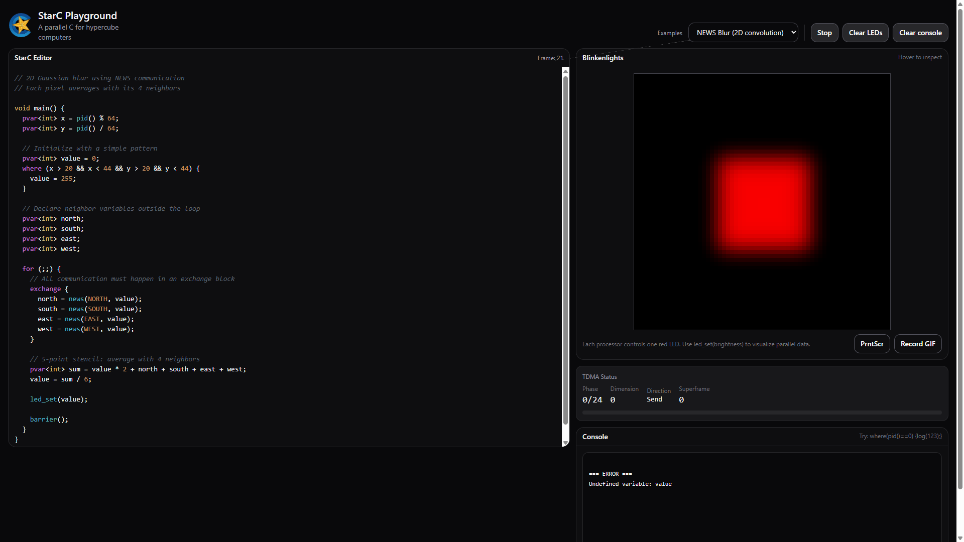
The playground has a dozen examples preloaded. There’s Conway’s Game of Life, dimension walks, LFSR scrolling columns, parallel Gaussian blurs, and examples of hypercube communications. Load one, hit run, and you’ll understand what StarC does faster than reading any specification.
StarC Identity
The name StarC is obviously inspired by the Connection Machine’s C* language. I got the starc-lang.org domain for cheap, and as a name for a language it’s good enough. The real inspiration was me going to a yakitori place on 8th and Clement in SF, right across the street from the Star of the Sea church. Stella Maris, the patron of sailors. Inside, there’s a shrine to the first millennial saint, the patron saint of programmers. I have ‘programmers’ and a concept of ‘sailors navigating the sea of a hypercube matrix’ all in one concept. You can’t turn down that kind of associative relationship. Cray has Chapel, I have a church.
But the StarC / Catholic iconography / sailor stuff is too good to ignore. I can do some cool Catholic iconography, or nautical imagery for the visual design of this language. I settled on a nautical star for the logo because of the relationship between sailors and the Star of the Sea church. With extra gradients in the art because I’m going for early 90s maximalism. The O’Reilly book should have a seahorse on the cover, because that’s how this specific Catholic iconography extends to the Animalia.
Get StarC
The full specification, with worked examples, the StarC Playground where you can run your own StarC programs on a virtual Thinkin Machine, and the links to the Python preprocessor with instruction on how to generate real C code can be found through the StarC website.
Calculating & Performance
Quantum Chromodynamics
G. Peter Lepage, “Lattice QCD for Novices,
Bitonic Sort
Neeural Network
Performance Vs. i7-12700K | RTX 5080
One More Thing
When I began this project, I imagined I’d be building an array of four thousand tiny ten-cent microcontrollers. These plans changed slightly as I worked through the architecture of the machine, and I eventually landed on a RISC-V and FPGA combo as the nodes in this massive machine. There are definite benefits to using these chips. They’re faster, they can do floating point arithmetic, they have more memory, and they’re the key to the TDMA messaging scheme I came up with.
But I’m really only using that FPGA portion of the chip as the communications interface for each chip. An FPGA can be anything. What if I used it to implement more processors?
The original Connection Machine CM-1 used 65,536 individual processors, and my machine uses 4,096. That’s a 16x difference. By implementing sixteen small cores in the FPGA of each node, I could extend my machine to match the number of processors in the original Connection Machine.
It’s a great idea. Because of how hypercubes partition, the sixteen new processors in each FPGA only need to talk to each other. The existing backplane handles everything between physical chips. And the original Connection Machine used very, very simple processors as the nodes – they could only process one bit at a time, and not many instructions were supported. It’s brilliant. Doing this, I’d have an exact reproduction of the original Connection Machine. It could have the original specification for each processor, and it could run the same code as the original. I could have the only working Connection Machine on the planet.
So that’s what I did.
Emulating the CM-1 on 4096 FPGAs
After reading Hillis’ thesis, we get a pretty clear picture of what the individual nodes in the CM-1 actually are:
- 1-bit datapath (bit-serial)
- 8 general-purpose flags + 8 special-purpose flags
- 4K bits of external memory (12-bit address)
- One instruction: read 2 memory bits + 1 flag, apply arbitrary 3-input boolean function (specified by 8-bit truth table), write 1 bit to memory + 1 bit to flag
- Conditionalization: execute or skip based on any flag
The 16 processors per chip in the original CM-1 were connected in a 4×4 NEWS grid AND via a daisy-chain. The 16 soft-cores per AG32 should form a 4D sub-hypercube (dimensions 0-3), with the physical AG32-to-AG32 connections handling dimensions 4-11.
All of this is covered in the CM-1 implementation page.
My “emulation” or “reimplementation” of the CM-1 – I’m not sure exactly what this is – has 65,536 1-bit processors all connected as a hypercube. The architecture is a bit different because the CM-1 used routers to pass messages around to the nodes, and I’m using a weird TDMA scheme so that each node is its own router. But still, this is the closest thing to a working connection machine that’s existed in the past two decades.
Theoretically, this machine could run original code for the Connection Machine. Maybe it could. I don’t actually know, because I can’t find any original CM-1 code. But if Danny wants to meet me for a beer at Interval, I would love to talk to him about this.
One More One More Thing
The comments section about this post will be lousy with questions of, ‘can you run an LLM on this?’. It’s a fair question, because you can run an LLM on a Commodore 64. Surely this machine could also be terrible at LLM inference.
Here’s where it gets weird: this machine, theoretically, is not terrible at running an LLM. Let’s go over what we have, and what we actually have to do to run an LLM:
- 4,096 RV32IMAFC cores, with hardware multiply (1 cycle).
- Each core has 64Mbit PSRAM.
- The communication between cores is through a hypercube toplogy, with 20 Mbps links between chips.
This is really interesting. A 7B model at FP32 is 28 GB, which fits in the 8 MB * 4,096 nodes. Each node holds 6.8 MB of local weights. An LLM inference is two operations: matrix multiply and reductions. Everything in a transformer forward pass is one of those two things. The matmul is very parallel, because we can split the weight matrix (by, say, putting it in 4,096 chips), each node multiplies its shard, and we’re done. Reductions are where this thing gets really cool. So let’s build it.
Building llama.starc
[2000 words of building the LLM inference thing, and there’s a video there showing it running – I’ll write this later.]
Why LLM Inference on Hypercubes Works
A hypercube is the optimal toplogy for reductions. Each reduction happens in log₂(N) hops, or 12 hops for my machine. Compare this to all-reduce on a GPU, which is sqrt(N) hops. That’s 64 hops for a GPU, 12 for this machine. To put some numbers behind this:
| Model | ||
|---|---|---|
| Parameters | 7B, FP32 | |
| Total weight size | 28 GB | 7B × 4 bytes |
| Weight per node | 6.84 MB | 28 GB ÷ 4,096 nodes |
| PSRAM per node | 8 MB | Fits, 1.2 MB left for activations |
| Compute | ||
| MACs per token | 7 billion | One multiply-accumulate per parameter |
| MACs per node | 1.71 million | 7B ÷ 4,096 (parallel) |
| Cycles per MAC | ~5 | Load, load, FMADD.S, store, loop |
| Compute time | 34 ms | 1.71M × 5 ÷ 248 MHz |
| Communication | ||
| All-reduces per token | 64 | 2 per layer × 32 layers |
| Hops per all-reduce | 12 | log₂(4,096) — the hypercube advantage |
| Data per all-reduce | 32 KB | Recursive halving-doubling, 4,096-element vector |
| Time per all-reduce | 13 ms | 32 KB × 8 bits ÷ 20 Mbps |
| Total communication | 838 ms | 64 × 13 ms |
| Result | ||
| Time per token | ~870 ms | 34 ms compute + 838 ms communication |
| Tokens per second | ~1.1 | |
One token per second doesn’t sound impressive until you consider the alternative. On a 2D mesh with 4,096 nodes — the topology every GPU and every AI accelerator on the market uses — those 64 all-reduces would take 64 hops each instead of 12. Same link speed, same data, 5.3× more communication time. The mesh version of this machine would generate one token every 4.7 seconds. The hypercube is doing the same work in a fifth of the communication time, because log₂(4096) is 12 and √4096 is 64. That’s what the topology gets you.
Now look at what’s actually slow. It’s not the processors — 34 milliseconds of compute is fine. It’s the 20 Mbps SPI links between chips on a backplane that was routed by an autorouter I wrote in my garage. Replace those wires with copper on a die — same topology, same TDMA schedule, same twelve hops — and the links go from 20 megabits to 20 gigabits. The 838 milliseconds of communication becomes 0.8 milliseconds. The architecture is identical. Only the wires change. I accidentally prototyped an LLM inference interconnect out of eighty-cent microcontrollers and a backplane that feels pain. The math says it’s the right topology. The Connection Machine was built to do AI. Forty years later, the same topology turns out to be optimal for the thing AI actually became.
I don’t want to put too fine a point on this, but this machine is what an ‘LLM inference box’ should look like. This toplogy, of sharding a model onto many cores, let the cores do matmul and have hypercube interconnects do the reductions, is the optimal topology for LLM inference. My machine can only do a token a second, but imagine if there were a ‘hypercube on a chip’ – a single silicon die with a huge amount of memory and just enough compute to do matmul and communicate over a hypercube toplogy.
I Would Like To Interact With The Literature
History says hypercubes as computers died because the USSR went tits up, or DARPA pulled funding, or because Moore’s law scaled enough and the Pentium was actually pretty good even with the FDIV bug, or because someone on Slashdot came up with the Beowulf cluster meme. These interpretations are in the shape of truth, but in academia, the hypercube died with Performance Analysis of k-ary n-cube Interconnection Networks by William J. Dally in an IEEE publication in 1990.
The thesis of this paper is that considering a VLSI wiring budget, hypercubes spend their wiring budget on many narrow links (hard to wire, and has limited bandwidth) versus other architectures with fewer, wider links (easier to wire, with more bandwidth). The wires are the computer, and in general, you will get more performance out of a machine with simpler, wider links between nodes.
This argument is plainly true; more bandwidth is always better. From experience, I can tell you that building a hypercube is hard. However, Dally’s argument is for general-purpose workloads. LLM inference is not a general-purpose workload. Inference is dominated by reductions, taking a value from every node and combining it into one, almost always a sum. Sharding that data across all nodes means a hypercube can reduce in log₂(N) hops, or 12 hops for an N=4096 machine. If this machine were laid out as a mesh, it would be √N, or 64 hops for a N=4096 machine. Twelve versus Sixty-four, and hypercubes only get better as the node count increases. Someone will point out you can run a tree all-reduce on a mesh and get logarithmic latency too, and they’re right. The difference is physical: on a hypercube each of those twelve steps is a single hop to a direct neighbor, while on a mesh the tree’s branches still have to cross the machine. The hypercube collapses logical and physical distance into the same thing. The mesh can’t. Yes, this math is a bit hand-wavey, but there are clear algorithmic advantages to doing LLM inference on a hypercube.
Imagine this entire machine shrunk down to a chip. It’s thousands of tiny cores, each with a slab of memory holding its weight shard, connected by on-die wires in a hypercube topology. Every core reads its local memory at full speed, does its multiply-accumulate, and the reductions propagate across the hypercube in nanoseconds. Compare this to what exists: Cerebras has 900,000 cores on a wafer-scale chip with a 2D mesh. A global reduction on their mesh takes √900,000 ≈ 949 hops. A hypercube with the same core count does it in log₂(900,000) ≈ 20 hops. That is a 47× reduction in communication latency for every all-reduce, every softmax, every layer norm, in every layer of every token. Tenstorrent is doing something similar but weirder, with a torus network. The market, or at least the funding, for an “LLM accelerator on a chip” is there.
The only open questions for this ‘hypercube on a chip’ are whether wiring a hypercube in nanometer-scale metal layers is even possible, and whether the pain of doing it is worth the algorithmic gains.
Back when Thinking Machines Corp. was still in business, Hillis believed the Connection Machine could be shrunk down into a chip. The Connection Machine was built for AI, and in the last few years we have a workload that is perfect for the Connection Machine’s architecture. This project proves the AI workloads of today can work on a machine from the mid-80s. Is it time to revisit this architecture? I don’t know, and I would appreciate feedback on whether a ‘hypercube on a chip’ could be a successful inference product. Or if it’s even possible. Either way, someone should build that chip.
Contextualizing the build
This project was insane, probably due to the mental space I was in while building it. Desperate soil yields desperate fruit, or something like that. This project began on month five of a 2-year long streak of unemployment, and if you’ve never been in that situation, I can’t convey how mentally taxing it is. Every day, for a few hours in the morning, I’d cruise LinkedIn, put in a few applications, and then spend the rest of my time working on this machine.
I got a few callbacks. Once every two months I’d have a company interested in me, have a second call, a third call, an interview with the team, and everything seems to go well. They like me. They call my references. My references say they like me. Then nothing. I thought about getting a Ouija board just so I can get some feedback.
Months of that - years of that - will tear you down. You become nothing. You are not useful. You are a burden to everyone else.
This project was my escape. Here, at least, I had some control. I could write some firmware for passing messages along the edges of a hypercube and at least I had some feedback because I have a logic analyzer on my desk. I’m serious when I say that were it not for this machine, I would not be here.
In previous roles that were heavily dependent on the engineering output of rogue garage tinkerers, I came up with the Bob Vila hypothesis. The idea goes something like this: In the mid-90s, someone asked Bob Vila why This Old House became a mainstay of public television. His answer? It was a recession. During the recession of the late 70s, people simply couldn’t afford to fix up old Victorians in Boston, so they did it themselves. They needed someone to show them how to remodel a kitchen, and which walls not to take out when renovating a room.
This theory can be extended to the incredible rise of amateur EE and MechE, with Arduinos and 3D printers and Maker Faires that coincided with the 2008 financial crisis. The dot com bubble had some really great software work despite Java. Going even further back Hewlett Packard was founded at the tail end of the depression.
So that’s the material conditions that led to me building this. It exists because of the environment that surrounds it. Not to distance myself too much from the work, but I really didn’t build this, I was just the conduit through which it was created. This is true for a lot of things; everything is a product of the environment it was created in.
This is how everything gets made. Take, for example, mid-century modern furniture. Eames chairs and molded plywood end tables were only possible after the development of phenolic resins during World War II. Without those, the plywood would delaminate. Technology enabled bending plywood, which enabled mid-century modern furniture. This was even noticed in the New York Times during one of the first Eames’ exhibitions, with the headline, “War-Time Developed Techniques of Construction Demonstrated at Modern Museum”.
In fashion, there was an explosion of colors in the 1860s, brought about purely from the development of aniline dyes in 1856. Now you could have purple without tens of thousands of sea snails. McMansions, with their disastrous roof lines, came about only a few years after the nail plates and pre-fabbed roof trusses; those roofs would be uneconomical with hand-cut rafters and skilled carpenters. Raymond Loewy created Streamline Moderne because modern welding processes became practically possible in the 1920s and 30s. The Mannesmann seamless tube process was invented in 1885, leading to steel framed bicycles very quickly and once the process was inexpensive enough, applied to the Wassily chair, a Bauhaus masterpiece, in 1925.
The Great Wave off Kanagawa was printed in 1831, and it couldn’t have been created much earlier. The blue of The Great Wave is Prussian blue, a synthetic pigment that didn’t exist before 1704. A shipment of Prussian Blue arrived in Japan in 1747, but it was sent back for some reason. Prussian Blue wasn’t used in Japan until 1752. By the time Prussian blue was readily available to Japanese printmakers in large quantities, Hokusai was carving the Great Wave. Two decades before the black ships arrived and Japan opened its ports to the world. The most famous piece of Japanese art exists because of European imports.
The point is, things exist because of the environment they were created in. And this Thinking Machine could not have been built any earlier.
The original Connection Machine CM-1 was built in 1985 thanks to advances in VLSI design, peeling a few guys off from the DEC mill, and a need for three-letter agencies to have a terrifically fast computer. It could only have been built in the 1980s, when VLSI fabs had spare capacity, DARPA had a budget to turn Moscow into glass, and the second AI boom made massively parallel anything look fundable. My machine had different factors that led to its existence.
The ten-cent microcontrollers that enabled this build were only available for about a year before I began the design. The backplane itself is a realization of two technologies – the CUDA pipeline that would make generating the backplane (and testing the code that created the backplane) take hours instead of months. Routing the backplane with a KiCad plugin would have been impossible without the IPC API, released only months before I began this project. The LED driver could have only been created because of my earlier work with the RP2040 PIOs and the IS31FL3741 LED drivers saved from an earlier project. And of course fabbing the PCBs would have cost a hundred times more if I ordered them in 2005 instead of 2025.
I couldn’t have built this in 2020, because I would be looking at four thousand dollars in microcontrollers instead of four hundred. I couldn’t have made this in 2015 because I bought the first reel of IS31FL3741s from Mouser in 2017. In 2010, the PCB costs alone would have been prohibitive.
The earliest this Thinking Machine could have been built is the end of 2025 or the beginning of 2026. I think I did alright. The trick wasn’t knowing how to build it, it’s knowing that it could be built. This is probably the best thing I’ll ever build, but it certainly won’t be the most advanced. For those builds, the technology hasn’t even been invented yet and the parts are, as of yet, unavailable.
Citations, Related Works, And Suggested Reading
-
bitluni, “CH32V003-based Cheap RISC-V Supercluster for $2” (2024).
A 256-node RISC-V “supercluster” built from CH32V003 microcontrollers. This was it, the project that pulled me down the path of building a Connection Machine. Bitluni’s project uses an 8-bit bus across segments of 16 nodes and ties everything together with a tree structure. Being historically aware, I spent most of the time watching this video yelling, “you’re so close!” at YouTube. And now we’re here. -
W. Daniel Hillis, “The Connection Machine” (Ph.D. dissertation, MIT, 1985; MIT Press, 1985).
Hillis’ thesis lays out the philosophy, architecture, and programming model of the original CM-1: 65,536 1-bit processors arranged in a hypercube, with routing, memory, and SIMD control all treated as one unified machine design. My machine is basically that document filtered through 40 years of Moore’s law and PCB fab: the overall hypercube topology, the idea of a separate “front-end” host, and the notion that the interconnect is the computer all trace back directly here. -
)William J. Dally, “Performance Analysis of k-ary n-cube Interconnection Networks,” IEEE Transactions on Computers, 39(6), 775–785 (June 1990).
The canonical “hypercubes are not free” paper. Dally shows that under a fixed VLSI wiring budget, high-dimensional binary n-cubes often lose to low-dimensional meshes and tori because the hypercube spends its wire budget on many narrow links instead of fewer wider channels. The counterargument here is that Dally analyzed general-purpose communication networks, while LLM inference is dominated by structured collectives — especially reductions — where a hypercube’s logarithmic diameter becomes the feature you are explicitly buying. -
Trammell Hudson, “CM-2 References” (2017). Bro got to pull cards out of cages, damn. Clarification on Random and Pleasing.
-
Thinking Machines Corporation, Connection Machine Model CM-2 Technical Summary, Version 6.0 (November 1990).
The official technical reference for the CM-2, covering everything from the virtual processor model to the function of the routers. The CM-2 was the production version of Hillis’s thesis; this manual is how they shipped it. -
Charles L. Seitz, “The Cosmic Cube,” Communications of the ACM, 28(1), 22–33, 1985.
Seitz describes the Caltech Cosmic Cube, a message-passing multicomputer built from off-the-shelf microprocessors wired into a hypercube network. Where Hillis pushes toward a purpose-built SIMD supercomputer, Seitz shows how far you can get by wiring lots of small nodes together with careful routing and deadlock-free message channels. This project sits very much in that Cosmic Cube lineage: commodity microcontrollers, hypercube links, and a big bet that the network fabric is the interesting part. -
W. Daniel Hillis, “Richard Feynman and The Connection Machine,” Physics Today 42(2), 78–84 (February 1989).
Hillis’ account of working with Feynman on the CM-1, including Feynman’s back-of-the-envelope router analysis, his lattice QCD prototype code, and his conclusion that the CM-1 would beat the Cosmic Cube in QCD calculations. -
Robert Schreiber, “An Assessment of the Connection Machine,” RIACS Technical Report 90.40 (June 1990) A clear-eyed, critique of the Connection Machine concept (specifically CM-2 as “a connection machine”): what it’s good at, where it hurts, and how its architectural/programming tradeoffs compare to contemporary MIMD multicomputers.
-
C. Y. Lee, “An Algorithm for Path Connections and Its Applications,” IRE Transactions on Electronic Computers, 1961.
The original maze-routing / wavefront paper: grid-based shortest paths around obstacles. Every “flood the board and backtrack” router is spiritually doing Lee; OrthoRoute is that idea scaled up and fired through a GPU. -
Larry McMurchie and Carl Ebeling, “PathFinder: A Negotiation-Based Performance-Driven Router for FPGAs,” in Proceedings of the Third International ACM Symposium on Field-Programmable Gate Arrays (FPGA ’95).
PathFinder introduces the negotiated-congestion routing scheme that basically every serious FPGA router still builds on. The OrthoRoute autorouter used to design the backplane borrows this idea wholesale: routes compete for overused resources, costs get updated, and the system iterates toward a legal routing. The difference is that PathFinder works on configurable switch matrices inside an FPGA; here, the same logic is being applied to a 32-layer Manhattan lattice on a 17,000-pad PCB and run on a GPU. -
G. Peter Lepage, “Lattice QCD for Novices,” Proceedings of HUGS 98, edited by J.L. Goity, World Scientific (2000); arXiv:hep-lat/0506036.
A practical introduction to lattice QCD with working code. Feynman’s original Connection Machine QCD program—written in a parallel Basic dialect he invented and hand-simulated—doesn’t survive, but the algorithm is standard Wilson action lattice gauge theory. Lepage’s paper provides the actual implementation. This is the benchmark: if my machine can run a simplified version of what Feynman was trying to do in 1985, it’s not just a replica. -
Hermann Kopetz and Günther Grünsteidl, “TTP—A Protocol for Fault-Tolerant Real-Time Systems,” IEEE Computer, 27(1), 14–23 (January 1994); first presented at FTCS-23, 1993. The foundational paper on the Time-Triggered Protocol. Kopetz’s insight—that a global time base and predetermined schedule can eliminate arbitration entirely—is the intellectual ancestor of the TDMA scheme used here. TTP/C now flies on the Orion spacecraft; the same core idea (the schedule is the coordination mechanism) makes a routerless hypercube possible.
-
Dimitri P. Bertsekas, Constantino Özveren, George D. Stamoulis, Paul Tseng, and John N. Tsitsiklis, “Optimal Communication Algorithms for Hypercubes,” Journal of Parallel and Distributed Computing, 11(4), 263–275 (1991). Formalizes dimension-ordered routing for hypercubes: always traverse dimensions in a fixed order and you get deadlock-free routing for free. Combined with time-triggered scheduling, this is how a 12-dimensional hypercube can operate without routers or arbitration logic.
-
Quentin F. Stout and Bruce Wagar, “Intensive Hypercube Communication: Prearranged Communication in Link-Bound Machines,” Journal of Parallel and Distributed Computing, 10(2), 167–181 (1990). Develops optimal algorithms for broadcast, permutation, and matrix transpose on link-bound hypercubes where all communication links can operate simultaneously. Stout assumes a working network and optimizes message patterns; the TDMA scheme here operates one layer down, using scheduling to create the collision-free network his algorithms assume.
-
Shridhar B. Shukla, “Scheduling Pipelined Communication in Distributed Memory Multiprocessors for Real-Time Applications,” ISCA ‘91, pp. 222–231 (1991). The grandfather of the whole idea. A compile-time schedule for a hypercube or torus, explicitly called “deadlock-free, contention-free, and does not load the intermediate node memory.” Shukla uses the phrase “time division multiplexing.” He cites Stout. He cites Bertsekas. The entire algorithmic content of my machine is sitting in one ACM paper from 1991, and almost nobody has touched it since.
-
Alan Edelman, “Optimal Matrix Transposition and Bit Reversal on Hypercubes: All-to-All Personalized Communication,” Journal of Parallel and Distributed Computing, 11(4), 328–331 (1991). The money sentence: “if every other node performs the same sequence of actions in its own relativized coordinate system, there will be no contention for communications channels.” Read in 2026 that’s a textbook description of TDMA. Read in 1991 it’s an algorithms paper about matrix transpose. Edelman ran it on a real CM-2; the Connection Machine was effectively executing collision-free schedules in 1990, it just paid for an expensive router to enforce them instead of letting the topology do it for free.
-
Shahid H. Bokhari, “Multiphase Complete Exchange on a Circuit Switched Hypercube,” NASA/ICASE Technical Report (1991); later in Parallel Processing Letters. All-to-all personalized communication on the Intel iPSC-860, scheduled as a sequence of partial exchanges on subcubes of varying dimension. So in 1991 there was a guy with hands on an actual circuit-switched commercial hypercube, running multi-phase scheduled communication, and writing it up for NASA. Nine years before Lee, Liu, and Jordan “proposed” the TDM hypercube.
-
Kyungsook Y. Lee, Guoping Liu, and Harry F. Jordan, “TDM Hypercube and TWDM Mesh Optical Interconnections,” Journal of Parallel and Distributed Computing, 60(11), 1337–1363 (2000). The paper that names the TDM-cube. log₂(N) time slots, fixed-wavelength transmitter per node, equations and block diagrams that map onto my schematic with embarrassing fidelity. Their machine was optical, hypothetical, and never built. Mine is microcontrollers, real, and on my desk. Same idea, twenty-six years apart.
-
Risto T. Honkanen, “Scheduled Routing in an Optical Hypercube,” ISPDC 2008, pp. 300–305. DOI: 10.1109/ISPDC.2008.16. A “systolic routing protocol based on cyclic changes of states of routers and scheduled sendings of packets” that guarantees “all packets injected into the routing machinery reach their targets without collisions.” Replace “optical” with “RS-232 at 2 Mbps” and “router” with “UART pin remap” and you have my project. Honkanen wrote a whole series of these between 2003 and 2010. Almost nobody cited them.
-
Chuck Thacker, “Hypercube Routing Scheme,” DEC SRC Technical Note 2000-001 (January 2000). Thacker independently arrives at bit-flip hypercube addressing and XOR-based routing in a small four-dimensional network, derived from first principles in a one-page memo. Reading this is what convinced me there is no original way to think about hypercubes. Everybody who works on one reinvents the same handful of tricks.
-
US Patent 5,420,982. “Hyper-cube network control system having different connection patterns corresponding to phase signals for interconnecting inter-node links and between input/output links.” Filed 1993, granted 1995, expired ~2015. The closest thing in the patent literature to what I’m doing. Bit train generator producing 2ⁿ phase signals, switching means selecting 2ⁿ connection patterns per phase, node designations where neighbors differ by one bit, control rule keyed on parity of 1-bits in the node ID. Every block diagram in this patent looks like a block diagram I drew. It expired without ever being commercialized, but you can’t unread it.
-
US Patent 5,367,636. “Hypercube processor network in which the processor identification numbers of two processors connected to each other through port number n vary only in the nth bit.” Filed 1989, granted 1994, expired. The addressing scheme of my machine, claimed verbatim. Up to 14 full-duplex I/O ports per node, dimensions to 13. Whatever you think you came up with, somebody at one of the big iron shops thought of it first and put it in a patent application.
-
US Patent 5,255,368. “Method for selecting data communications paths for routing messages between processors in a parallel processing computer system organized as a hypercube.” Filed 1991, granted 1993, expired. Claim 1 spells out the routing algorithm: “form a distance by exclusive or-ing a starting node address with destination node address,” then walk the differing bits. Strip the patent-attorney prose and that’s a
forloop you’d write at 2am. -
US Patent 4,814,980. “Concurrent hypercube system with improved message passing.” Filed 1986, expired ~2006. The hardware skeleton: bidirectional links per dimension, FIFO at each node, a clocking line between neighbors, supervisory signals indicating FIFO empty/full. There’s a 1986 patent that already covered the physical layer of what I’m building, twenty years before the parts I’m using even existed.
-
US Patent 6,456,588. “Hypercube routing and restoration in telecommunications networks.” Filed 1997, granted 2002, expired ~2017. XOR-based hypercube routing for telecom failover. Different application, same algorithm. Sleeping in a patent file for two decades.
-
Hayashi et al., US 4,918,626 / US 5,339,396 / US 5,517,619 (Hitachi, priority 1987–1988, all expired); related Japanese application JP 2512661B2 covering non-binary hypercubes. The Hitachi family. Crossbars and interconnects for parallel processors with various flavors of hypercube switching. None of these is exactly what I’m doing, but together they cover most of the territory around it. Read the file wrappers and you can see every place I would have collided with a portfolio had I tried this in 1995.
-
Hermann Kopetz, Real-Time Systems: Design Principles for Distributed Embedded Applications, Kluwer Academic Publishers (1997). ISBN 978-0792398943. If TTP/C is the paper, this is the book. Kopetz lays out the entire theory of time-triggered architectures — global time base, sparse-time model, static schedule, fail-silent components — over 300 pages. Read this before you build any kind of deterministic distributed system, because Kopetz has thought about your edge case already.
-
Gerardine Leen and Donal Heffernan, “TTCAN: A New Time-Triggered Controller Area Network,” Microprocessors and Microsystems, 26(2), 77–94 (2002). The canonical TTCAN paper. CAN bus plus a TDMA matrix cycle for deterministic timing in automotive control. Capped at 1 Mbit/s with limited cable length, but the schedule concept is identical to what I’m doing on a different physical layer. Worth reading just to see how the automotive industry quietly solved this thirty years ago and called it Tuesday.
-
Hermann Kopetz, Astrit Ademaj, Petr Grillinger, and Klaus Steinhammer, “The Time-Triggered Ethernet (TTE) Design,” ISORC 2005; now standardized as SAE AS6802. TTEthernet. TDMA on top of Ethernet, scheduled by switches that know the global time. Now flies on the Orion spacecraft. The aerospace world solved the deterministic-distributed-systems problem a long time ago using exactly the trick I’m using; I just have a different topology underneath and a smaller budget.
-
Kees Goossens, John Dielissen, and Andrei Rădulescu, “Æthereal Network on Chip: Concepts, Architectures, and Implementations,” IEEE Design & Test of Computers, 22(5), 414–421 (2005); and Kees Goossens and Andreas Hansson, “The Æthereal Network on Chip after Ten Years: Goals, Evolution, Lessons, and Future,” DAC 2010. The on-chip TDM network from Philips/NXP. Per-slot connection tables in each router, contention-free routing, no arbitration logic. Goossens and team spent a decade shipping this in real silicon. Different topology from a hypercube, same fundamental abstraction: precompute the schedule, throw away the routers. The 2010 retrospective is the playbook for shipping a TDM network in silicon.
-
Quentin F. Stout and Bruce Wagar, “Intensive Hypercube Communication: Prearranged Communication in Link-Bound Machines,” Journal of Parallel and Distributed Computing, 10(2), 167–181 (1990); preliminary version in Hypercube Multiprocessors 1987. The paper. “Communication pattern known in advance by all processors, all messages are of the same size, message headers are not needed because all nodes know the task being performed, and all nodes can use all communication links simultaneously.” That is, to a comma, the algorithmic content of my machine — written in 1987, published in 1990, and almost completely ignored for thirty-five years. Stout assumed a working network and optimized message patterns; I’m using his optimization to design the network in the first place.
Prior Art (Or: How I Learned to Stop Worrying and Love the TDM‑cube)
You didn’t think I was the first person to think of this, did you? Of course not. The idea of a time‑division multiplexed hypercube has been kicking around the literature for three decades. Let me save you the deep‑dive and tell you what’s out there.
The TDM‑cube (2000)
In 2000, Kyungsook Y. Lee, Guoping Liu, and Harry F. Jordan published a paper in the Journal of Parallel and Distributed Computing titled “TDM Hypercube and TWDM Mesh Optical Interconnections”. They defined the TDM‑cube(N) as a network that “implements the binary hypercube interconnection among N nodes in log₂(N) time slots.” That’s exactly my TDMA scheme, described in equations and block diagrams.
Their paper was about optical interconnects – lasers, waveguides, the whole deal. They never built a chip, never wrote a line of firmware, and certainly never ran an LLM. A handful of other papers cite them (Wang 2003, Abdelhalim 2010, a few Chinese dissertations). All of them are simulations or optical modeling. Zero hardware.
Scheduled Routing (1991)
Way back in 1991, Shridhar B. Shukla presented a paper at ISCA called “Scheduling pipelined communication in distributed memory multiprocessors for real‑time applications.” He proposed “scheduled routing” and explicitly said it was “deadlock‑free, contention‑free, and does not load the intermediate node memory.” That’s the same trick – a compile‑time schedule for a hypercube or torus. He even used the phrase “time division multiplexing.”
Shukla’s work is the true grandfather of this idea. It was cited by Lee et al. and by a few real‑time systems papers. Again, no one ever built it.
The Expired Patent (1993)
This one stung a little. US Patent 5,420,982 – “Hyper‑cube network control system having different connection patterns corresponding to phase signals” – was filed in 1993 and granted in 1995. It describes a hypercube where each node has a “device for setting 2ⁿ different connection patterns corresponding to 2ⁿ phase signals.” The drawings could pass for my block diagram.
The good news: the patent expired around 2015. The bad news: it means the basic idea of a TDMA hypercube was patented thirty years ago. The great news: no one ever commercialized it, and my specific implementation (RISC‑V + FPGA fabric, LLM inference, 20 Mbps backplane, the whole shebang) is nowhere in that patent. You can’t patent the concept – but you can patent what you actually built.
What Was Missing
Every single one of these prior works stayed on paper. No one fabricated a chip. No one assembled 4,096 nodes. No one wrote a TDMA mux in Verilog and stuffed it into an eighty‑cent microcontroller. No one ran a neural network. The idea was a mathematical curiosity, not a machine.
That’s where I came in.
So What’s New?
| Prior art (theory) | This machine | |
|---|---|---|
| TDMA hypercube | Lee, Liu, Jordan 2000; Shukla 1991; US 5,420,982 | Yes – but now it’s physical |
| Hardware implementation | None | 4,096 AG32 nodes, backplane, blinking LEDs |
| LLM inference | None | 7B model, 1.1 token/sec, O(log n) all‑reduce |
| Open source toolchain | None | Python bitstream generator, KiCad files, StarC compiler |
So no, I didn’t invent the TDMA hypercube. But I’m the first person to prove it works in silicon, and the first to show it’s the optimal topology for the most important workload of the decade. That’s not nothing.
Citations for the curious:
- Lee, K.Y., Liu, G., & Jordan, H.F. (2000). TDM Hypercube and TWDM Mesh Optical Interconnections. JPDC, 60(11), 1337–1363.
- Shukla, S.B. (1991). Scheduling pipelined communication in distributed memory multiprocessors for real‑time applications. ISCA ’91, 222–231.
- US Patent 5,420,982 (expired). Hyper‑cube network control system… (1995).
Prearranged Communication (1987–1991) Then it got worse. Quentin Stout and Bruce Wagar at Michigan wrote a paper called “Intensive Hypercube Communication: Prearranged Communication in Link‑Bound Machines” that appeared in JPDC in 1990, but they’d presented a preliminary version at the Hypercube Multiprocessors conference in 1987. Read the abstract slowly: “the communication pattern is known in advance by all processors, all messages are of the same size, message headers are not needed because all nodes know the task being performed, and all nodes can use all communication links simultaneously.” That is, to a comma, the algorithmic content of what I’m doing. They didn’t use the word “TDMA” because they were hypercube algorithms people, not telecom people. They didn’t build a chip. They just proved the schedule works and went home. A year later Alan Edelman at Berkeley published “Optimal Matrix Transposition and Bit Reversal on Hypercubes: All‑to‑All Personalized Communication” [JPDC 11, 1991], which contains the sentence: “if every other node performs the same sequence of actions in its own relativized coordinate system, there will be no contention for communications channels.” That’s the property the whole TDMA scheme exploits. Every node runs the same phase counter, the bit‑flip neighbor structure guarantees nobody steps on anybody, and you get a routerless, collision‑free hypercube for free. Edelman implemented it on a real CM‑2 — so the Connection Machine itself was already running collision‑free schedules in 1990, just paying for an expensive router to do it. Same year, Bertsekas, Özveren, Stamoulis, Tseng, and Tsitsiklis dropped “Optimal Communication Algorithms for Hypercubes” [JPDC 11, 1991], which is the paper that formalizes dimension‑ordered routing as the way you walk a hypercube without deadlocking. Combine Stout’s prearranged schedule with Bertsekas’s dimension ordering and you have, on paper, in 1991, the entire mathematical content of routerless hypercube communication. Nobody owes me any credit for the idea. And then there’s Bokhari [NASA/ICASE 1991], whose paper “Multiphase Complete Exchange on a Circuit Switched Hypercube” describes multi‑phase scheduling of partial exchanges on hypercube subcubes — and actually implemented it on an Intel iPSC‑860, a real circuit‑switched commercial hypercube. So Lee, Liu, and Jordan in 2000 weren’t even the first to propose a time‑multiplexed hypercube. They just put it in optics and gave it a name. The Rest of the Patent Pile The 5,420,982 patent isn’t the only one I should be sweating. While I was checking that it had really, definitely expired (it has), I went looking for siblings. There are several. US 5,367,636 (1989 priority, granted 1994, expired): “Hypercube processor network in which the processor identification numbers of two processors connected to each other through port number n vary only in the nth bit.” That’s the entire addressing scheme of my machine, claimed verbatim, with up to 14 full‑duplex I/O ports per node and dimensions up to 13. US 5,255,368 (1991 priority, granted 1993, expired) claims a hypercube where each node has one bidirectional path per bit position of its binary address, and routes by “forming a distance by exclusive or-ing a starting node address with destination node address” and walking the differing bits in order. That’s how my nodes pick the next hop. US 4,814,980 (1986 priority, expired ~2006) claims the hardware skeleton — bidirectional links, FIFOs, clocking line between neighbors, status signals. US 6,456,588 (1997 priority, granted 2002, expired ~2017) does XOR‑based hypercube routing for telecoms. There’s also a Hitachi family from Hayashi et al. (US 4,918,626 / 5,339,396 / 5,517,619) going back to a 1987 priority date that covers a chunk of the crossbar interconnect territory, and JP 2512661B2 in Japanese covers non‑binary hypercubes. All expired. Every one of them. The good news is I can use it. The bad news is the territory was claimed, mapped, and abandoned thirty years ago. The Time‑Triggered Cousins The broader idea — global clock plus precomputed static schedule, eliminating arbitration — has been the dominant solution in safety‑critical real‑time systems since the early 90s. Kopetz and Grünsteidl’s TTP/C (IEEE Computer, 1994). TTCAN (Leen and Heffernan, 2002), which is “put TDMA on top of CAN bus and call it deterministic.” TTEthernet (Kopetz, Ademaj, Grillinger, Steinhammer, ISORC 2005, now SAE AS6802), which is “put TDMA on top of Ethernet.” The whole TSN / IEEE 802.1 family, which is the industrial Ethernet umbrella. And on chip: the Æthereal NoC (Goossens et al., Philips/NXP, 2003 onward), a TDM router with per‑slot connection tables, contention‑free routing, no arbitration logic — they wrote a ten‑year retrospective in 2010 that more or less is the playbook for shipping a TDM network in silicon. None of these are hypercubes. They’re buses, switches, meshes. But the abstraction — time‑triggered, schedule‑driven, contention‑free — is the same one I’m using. The hypercube is what makes the schedule cheap (12 dimensions × 2 directions = 24 phases and you’re done). The schedule is what makes the hardware cheap (no routers). Both halves have been in the literature for thirty years. Stack them together and you get this machine. So What’s Actually New Honestly? Nothing about the idea. The TDMA hypercube has been patented (expired), described (in detail), implemented in optics (Lee/Liu/Jordan, Honkanen), and proved correct in algorithms papers (Stout, Edelman, Bertsekas, Bokhari). The bit‑flip addressing, dimension‑ordered routing, XOR‑distance routing, time‑triggered scheduling, routerless hypercube communication — all of it predates me by three decades and change. What’s new is that nobody actually built one out of cheap commodity microcontrollers. Lee, Liu, and Jordan modeled it in optics. Stout proved the schedule. Shukla designed the timing. The 5,420,982 patent describes a switching system that never got reduced to practice. Honkanen explored optical variants. None of them put 4,096 RISC‑V chips on a backplane and ran a neural network on it, because in 1991 the per‑node BOM cost would have been four thousand dollars instead of forty cents. The contribution here is the build, the toolchain (StarC, OrthoRoute), and the fact that this machine exists and runs code. Not the architecture. Not the routing scheme. The contribution is that the price of a RISC‑V plus a tiny FPGA fabric fell below a dollar in 2025, and somebody had to be the person to notice that the prior art had been waiting thirty years for the bill of materials to catch up. That’s enough. It doesn’t need to be patentable to be worth doing.