
A 16 Node Hypercube Microcontroller Cluster
The original inspiration for this build is bitluni’s CH32V003-based Cheap RISC-V Supercluster for $2. This is a fantastic build that uses ten cent microcontrollers as a parallel computer.
The only problem with bitluni’s build is that it is not historically literate. There are better ways to arrange a handful of really cheap microcontrollers than simply putting them on an 8-bit bus. A ten cent microcontroller might not have a lot of processing power, but there are different network topologies that are much more interesting than a big fat bus. Want a pseudo-token ring network? That’s possible. A 4x4 mesh, like the early Intel Paragon? Easy. A torus, wrapping the mesh around so the edges connect? A few more wires. A binary tree, like the INMOS Transputer setups? Sure, if you’re okay with the root being a bottleneck. A butterfly network for FFT-style computation? Doable. A systolic array, like a Google TPU? That’s just a mesh with a rhythm.
But no. There’s one network topology that is the best choice for a pocketful of silicon in the form of RISC-V microcontrollers. A hypercube. Build a Connection Machine. The original had 65,536 processors arranged in a 16-dimensional hypercube, with each processor connected to exactly 16 neighbors. It’s in the New York MoMA. It’s got blinkenlights. It’s in Jurassic Park. You could only program it with Lisp. It’s really, really weird.
…So that’s what I’m doing. I’m building a Connection Machine out of a bunch of cheap RISC-V microcontrollers. This is the first step. Sixteen microcontrollers arranged as a hypercube.
Architectural Limitations
The hypercube architecture of this is simple. Use single-wire serial links to connect dozens, hundreds, or thousands of microcontrollers together. This is, in theory, easy. But there are some caveats.
- Chips don’t have UARTs on all pins – A hardware UART, where a specific bit of silicon handles the mechanics of sending and receiving data from other chips, would be really helpful for this project. A hypercube architecture can be done without these hardware UARTs, specifically by ‘bit banging’ the serial connections between chips. But this is hard to code and won’t perform as well as a hardware UART.
- How do I program these things? – These microcontrollers will have to be programmed externally by another chip. I could put programming headers next to each node in the hypercube, but with a few extra chips I could also use another, larger microcontroller to do this automatically
- A synchronous clock and reset – bitluni’s supercluster used the internal clock for all nodes in his machine. While the internal clock in the CH32V003 is nominally 48MHz, there’s a small amount of drift. This means chips will eventually fall out of synchronization with each other. I can accomplish this with an external clock piped to all nodes in the supercluster. A reset signal can also be sent to all nodes simultaneously, so they all start at the same time.
The second and third problems are solved relatively easily. For the ‘control microcontroller’, I’m using a Raspberry Pi Pico and can leverage the PIOs to generate clock signals. I’ve done this before, and it’s a great way to generate clock signals from 32kHz to 4MHz. To toggle the Boot0 and Reset signals of the hypercube nodes, I can use a GPIO expander. They’re cheap and will do the job. For serial, I can broadcast TX from the control microcontroller to every other chip and use an analog mux to read all the RX signals from the nodes in the hypercube. That means I can’t read serial from all the chips at the same time, but it’s simple enough to be basically foolproof and cheap for a prototype.
The problem of the node microcontrollers not having UARTs on all the pins is a big one. Ideally, we can use hardware UARTs in the hypercube nodes to speak to every other chip. The CH32V003 and the larger CH32V203 only have two hardware UARTs. One will be dedicated to the control microcontroller. The other? It’s basically unusable in this instance. So if I use CH32V203 chips as the nodes in a hypercube, I’ll have to bitbang the serial connections between all hypercube links.
But there’s another chip that makes this entire machine better. The AG32 SoC has a RISC-V microcontroller core and a 2k LUT FPGA in a single package. It costs eighty cents in quantity. With the FPGA, I can create a small system that automatically routes data anywhere despite the RISC-V microcontroller only having a handful of hardware UARTs. This is the ideal chip for this machine. It will just work with the hypercube architecture.
But the AG32 chip carries a significant amount of risk with Chinese docs, a weird toolchain, and the fact that I would be the first English-speaking person working with this chip. Most of that risk isn’t related to the combination hypercube / tree architecture I’m planning.
The plan is this: I’ll build a 16-node prototype with the CH32 chips, verifying the clock distribution, independent programming, and play around with a bitbanged UART, just to see if it’s possible. If that works, I’ll do it again with the better AG32 chip. I’ll create an FPGA implementation of a hypercube UART. If all goes well, I’ll have two prototypes, one with a bitbanged hypercube UART, and another with FPGA hypercube connections.
One of them will probably work. Let’s dig in.
The CH32V203 Board
I’ll be building two of these, one using the CH32V203 as the nodes in a 16-node hypercube, the other using the AG32 as the nodes in a hypercube.
Control Microcontroller
The control microcontroller is the ‘master’ of the system. It’s the hypercube’s interface to the outside world. It’s how the nodes in the hypercube are programmed. For this, I’m using a Raspberry Pi RP2040. It’s capable enough, dual-core, and it has PIOs to generate clock signals. The ‘base’ circuit is pretty much a rip off of the Raspberry Pi Pico:
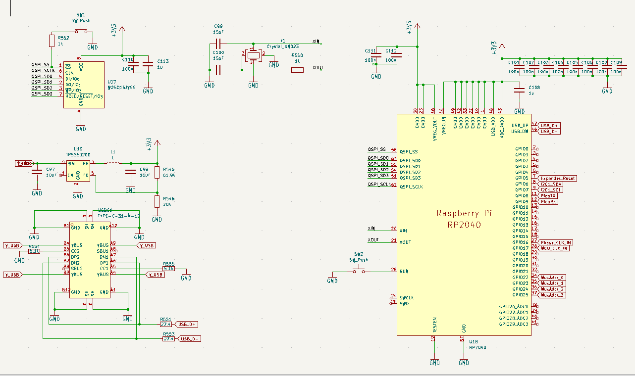
The RP2040 requires an external Flash chip, I’m using the W25Q16JVSS for 16 Megabits or 2 Megabytes of storage. Power is provided through a USB C connector, stepped down to 3.3V for the entire system through a TPS560200 step-down regulator. Add buttons for boot and reset, and this is effectively a copy of the Raspberry Pi Pico.
The Node Microcontroller
Each of the nodes in the hypercube are based on the CH32V203. I’m using this chip instead of the CH32V003 because it’s more capable and easier to integrate into a full system; the /RST and Boot0 pins are easier to ping on the CH32V203, and clocking is easier. The price difference between the chips isn’t really significant, thirteen cents for the ‘003 and thirty-two for the ‘203.

Each node uses PA9 and PA10 for the UART connection to the master microcontroller. The bootloader for this chip allows for code to be uploaded over this port. The ‘dimension connections’ are through PA2, PA3, PA4, and PA5. These pins connect to other dimensions in the hypercube.
A 4D hypercube has a specific topology. Node 0 connects to nodes 1, 2, 4, and 8. Node 5 connects to 4,7,1, and 13. Each dimension connection links to the node whose address differs by exactly one bit. D0 flips bit 0, D1 flips bit 1, and so on. A complete mapping is shown in this table:
| Node | Binary | D0 (PA2) | D1 (PA3) | D2 (PA4) | D3 (PA5) |
|---|---|---|---|---|---|
| 0 | 0000 | 1 | 2 | 4 | 8 |
| 1 | 0001 | 0 | 3 | 5 | 9 |
| 2 | 0010 | 3 | 0 | 6 | 10 |
| 3 | 0011 | 2 | 1 | 7 | 11 |
| 4 | 0100 | 5 | 6 | 0 | 12 |
| 5 | 0101 | 4 | 7 | 1 | 13 |
| 6 | 0110 | 7 | 4 | 2 | 14 |
| 7 | 0111 | 6 | 5 | 3 | 15 |
| 8 | 1000 | 9 | 10 | 12 | 0 |
| 9 | 1001 | 8 | 11 | 13 | 1 |
| 10 | 1010 | 11 | 8 | 14 | 2 |
| 11 | 1011 | 10 | 9 | 15 | 3 |
| 12 | 1100 | 13 | 14 | 8 | 4 |
| 13 | 1101 | 12 | 15 | 9 | 5 |
| 14 | 1110 | 15 | 12 | 10 | 6 |
| 15 | 1111 | 14 | 13 | 11 | 7 |
A 4k7 resistor pulls Boot0 to ground per the datasheet, and PB7 is used for an LED. It’s gotta have some blinky, right?
The Clock Tree
The microcontrollers in the hypercube need to run in lock step with each other. The CH32V203 supports running from an external oscillator, so the problem is just sending a ~4MHz clock to each chip. I’m doing this with a tree of 74LVC1G17 Schmitt-trigger inputs, used as buffers. These are arranged in a tree. One 741G17 drives the clock for four different hypercube microcontrollers, and these are driven by another 741G17 coming from the RP2040. Each 741G17 only drives four other clock sinks.
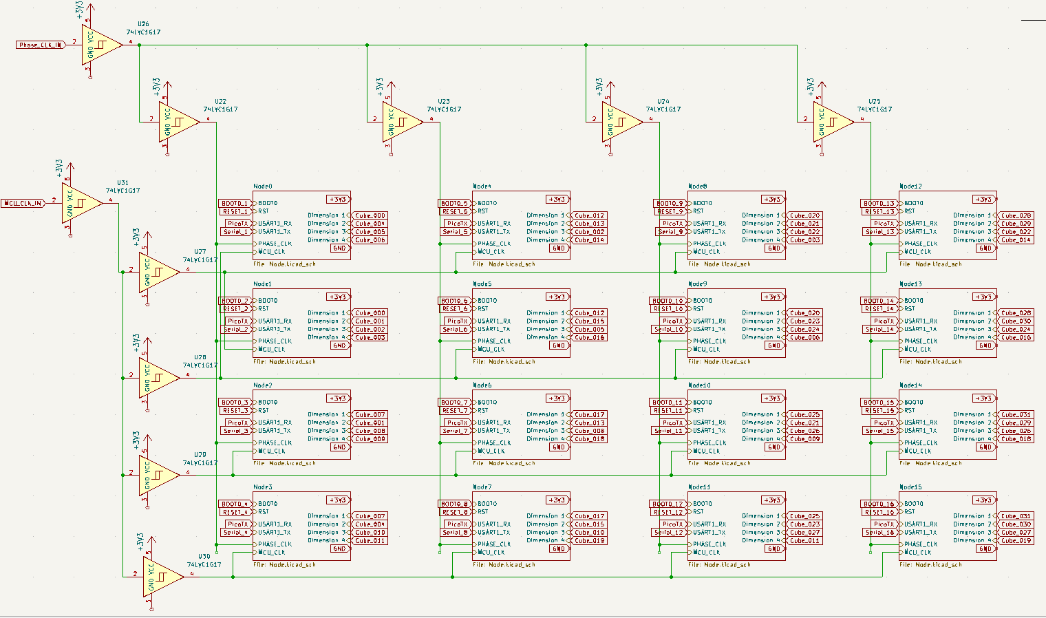
Additionally, each chip requires a second clock, running somewhere between 10kHz and 100kHz. This signal will be used for a TDMA message passing scheme. If you’re reading the pages for this build log in the right order, you will know this second clock is the critical insight that makes this entire machine possible. This clock is also generated by the RP2040, and sent out to the hypercube microcontrollers with an identical 741G17 clock tree.
Boot0 and /RST
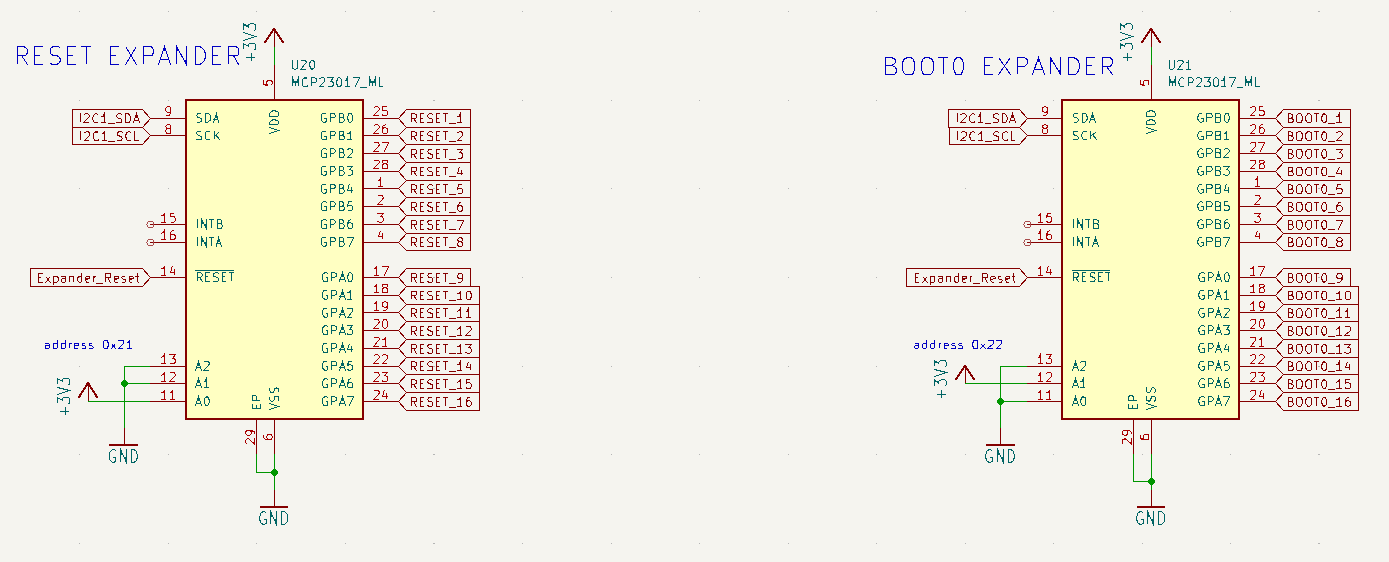
To program the CH32V203 over a UART, the bootloader requires pulling the Boot0 to +3V3 and /RST pins to ground. For 16 individual chips, this requires 32 GPIO outputs on the RP2040. I’m doing this with the MCP23017, an I2C GPIO expander, providing 16 GPIO outputs. The Boot0 connections to each hypercube node gets one of these expanders, the /RST gets a second:
The Serial Mux
Now we’re getting into the fundamental limitations of modern silicon. The ‘control microcontroller’ is the master of the entire system, and connects to each node over a hardware UART. There are no microcontrollers with sixteen independent hardware UARTs, so we’ll have to mux them somehow.
The solution I came up with is to broadcast the TX from the RP2040 to all nodes in the hypercube at once. To receive data from each node on the RP2040, I’m using an analog mux, specifically the 74HC4067. This device will take the TX from each of the nodes in the hypercube, with the common attached to the RX on the RP2040. This chip is controlled over GPIO, so it’s simple enough to wire up.

The drawback of this architecture is that the RP2040 can only communicate with one node chip at a time. That’s fine; since I’m also controlling the Boot0 and /RST lines independently, I can program all the nodes sequentially. It’s not ideal, but it will work for a prototype.
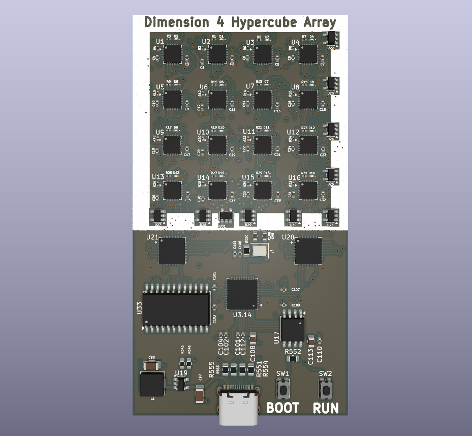
The Finished CH32V203 Board
The prototype board is 4 layers, 93mm by 47mm:
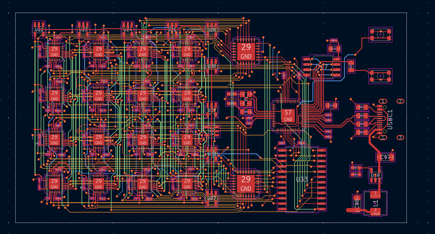
Routing this was a pain. But not too bad, because I used horizontal traces on layer 2 and vertical traces on layer 3, using the top and bottom for power and ground. This is exactly the idea I used for OrthoRoute, the ‘GPU accelerated Manhattan router’ used to route the backplane for the full 4,096-node backplane.
I bought two of these boards, assembled, from JLCPCB. Total costs were:
| Line Item | Cost |
|---|---|
| Boards | 4.20 |
| Assembly | 116.07 |
| Shipping | 50.81 |
| Import Taxes | 50.08 |
For a total cost of Two hundred and twenty-six dollars. This is all tariffs and Trump. This sucks, man, this really sucks.
Bringup of CH32V203 Board
….something about the bringup, actual code…
The AG32VF303 Board
AGM MICRO STUFF:
The AG32 SoC is offered in sizes ranging from a QFN32 to a huge LQFP100 package. Size is a constraint in this board, and I really only need a handful of GPIOs. I’m using the QFN32 part, the AG32VF303KCU6